Electron bombardment of wide bandgap semiconductors for generating high brightness and narrow energy spread emission electrons

a wide bandgap semiconductor and electron beam technology, applied in the direction of discharge tube/lamp details, discharge tube luminescnet screen, discharge tube main electrode, etc., can solve the problem of limiting the applicability of many of these devices, the photocathode that operates with available light sources and optics is very sensitive to contamination, and the standard cathode cannot deliver such high brightness beams with the requisite narrow energy spread, etc. problem, to achieve the effect of small emission electron energy

Inactive Publication Date: 2006-02-28
THE BOARD OF TRUSTEES OF THE LELAND STANFORD JUNIOR UNIV
View PDF9 Cites 6 Cited by
  • Summary
  • Abstract
  • Description
  • Claims
  • Application Information

AI Technical Summary

Benefits of technology

[0020]The invention further provides a method for obtaining emission electrons from the target by controlling the energy of the seed electrons and selecting the thickness of the target. These two parameters are adjusted such that the emission electrons from the fraction of the electron-hole pairs which provide them, are substantially thermalized at the emission surface. The more complete the thermalization of emission electrons at the emission surface, the smaller the energy spread of the emission electrons in the beam of emission electrons. It is also important that the target thickness is thin enough to prevent significant electron-hole recombination, which acts to red

Problems solved by technology

Recent requirements for high brightness (defined as current density per solid angle) and narrow energy spread of the electrons constituting the beam seriously limit the applicability of many of these devices.
Standard cathodes are not capable of delivering such high brightness beams with the requisite narrow energy spread because the electron emission conditions in a typical cathode are difficult to control, inherently noisy and the cathodes are not sufficiently robust.
In the case of photocathodes, photocathodes that operate with available light sources and optics are very sensitive to contamination.
Photocathodes which promise to be more robust lack available light sources delivering photons of apropriate energy to operate the photocathodes to produce such high brightness and nar

Method used


Image

  • Electron bombardment of wide bandgap semiconductors for generating high brightness and narrow energy spread emission electrons
  • Electron bombardment of wide bandgap semiconductors for generating high brightness and narrow energy spread emission electrons
  • Electron bombardment of wide bandgap semiconductors for generating high brightness and narrow energy spread emission electrons

Examples


Embodiment Construction

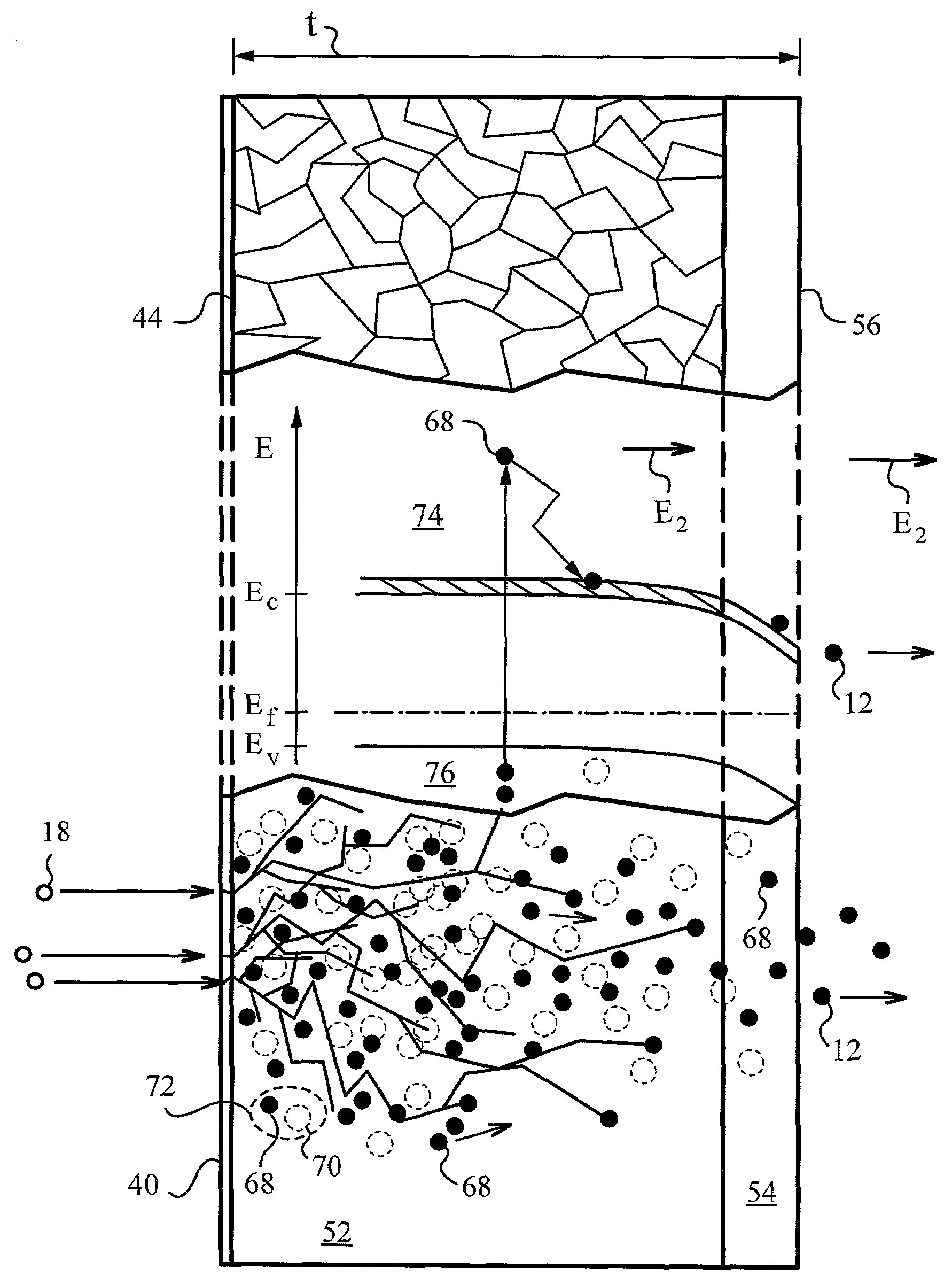
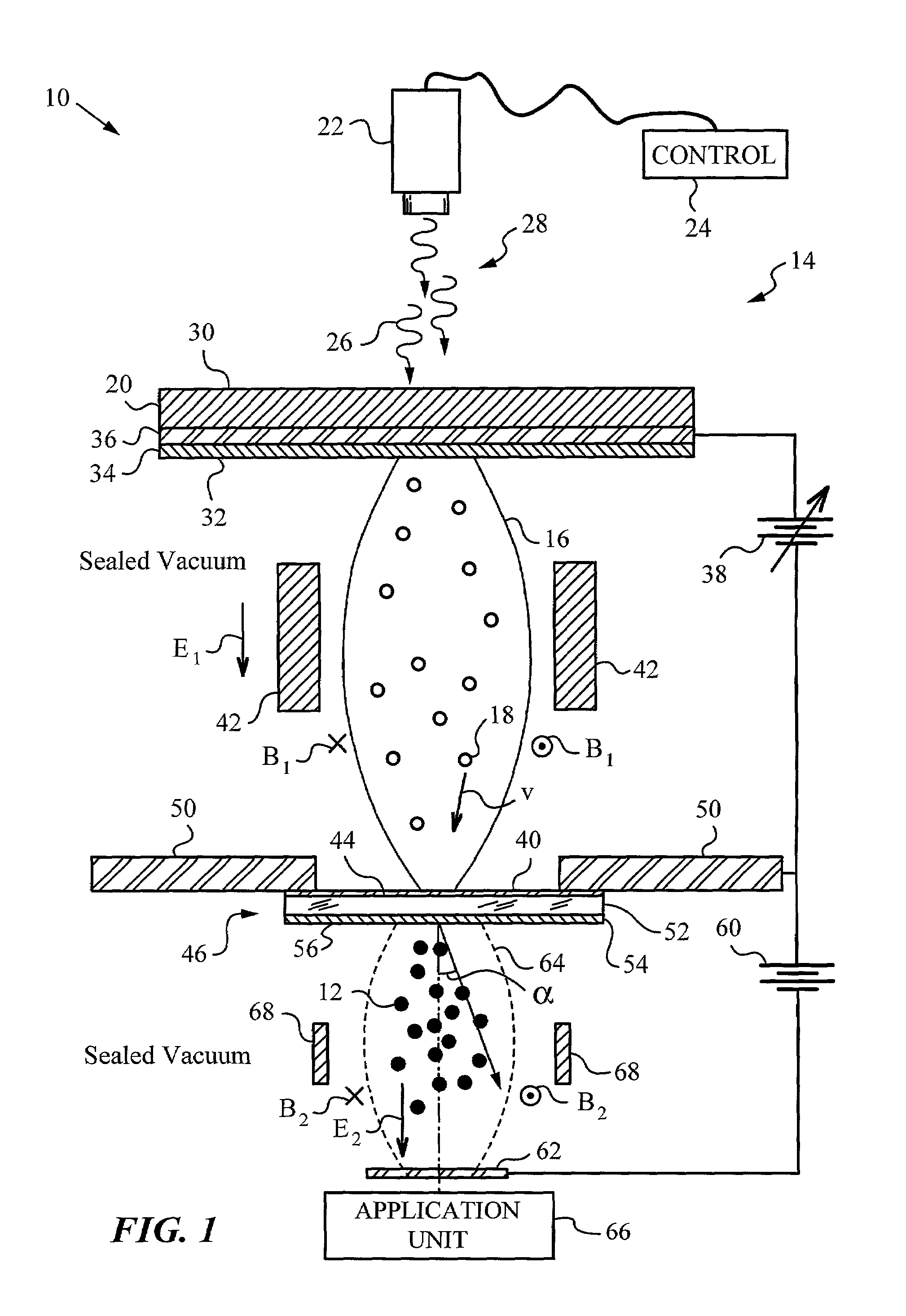
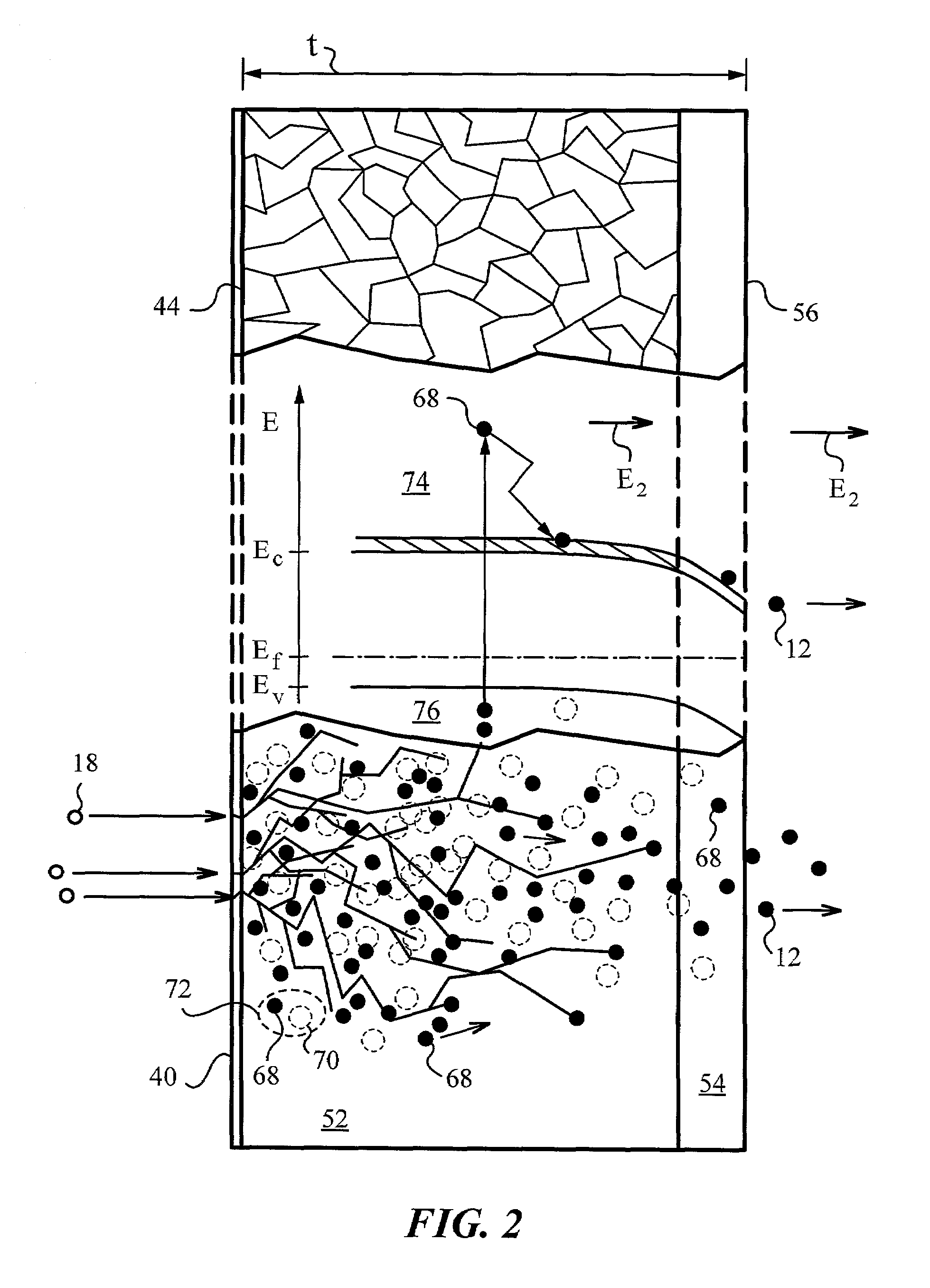
[0026]FIG. 1 illustrates in a plan schematic diagram a preferred embodiment of a wide bandgap semiconductor source 10 of emission electrons 12. Source 10 has an arrangement 14 for producing and directing a beam 16 of seed electrons 18 at a target 46 mounted on a stage 50. Target 46 contains a layer of wide bandgap semiconductor 52 selected to produce and release emission electrons 12 under bombardment with beam 16 of seed electrons 18. For the purposes of this invention wide bandgap semiconductor 52 has a bandgap of at least 1.9 eV.

[0027]In the present embodiment, arrangement 14 includes a photocathode 20 and a light source 22 controlled by a control unit 24. Light source 22 can be a laser, a lamp or any other suitable source capable of producing photons 26 of sufficient energy to cause photoinduced generation of seed electrons 18 in photocathode 20 upon illumination with a light beam 28 containing photons 26. It will be appreciated by a person skilled in the art that any appropriat...


PUM


Abstract

A semiconductor source of emission electrons which uses a target of a wide bandgap semiconductor having a target thickness measured from an illumination surface to an emission surface. The semiconductor source is equipped with an arrangement for producing and directing a beam of seed electrons at the illumination surface and a mechanism for controlling the energy of the seed electrons such that the energy of the seed electrons is sufficient to generate electron-hole pairs in the target. A fraction of these electron-hole pairs supply the emission electrons. Furthermore, the target thickness and the energy of the seed electrons are optimized such that the emission electrons at the emission surface are substantially thermalized. The emission of electrons is further facilitated by generating negative electron affinity at the emission surface. The source of the invention can take advantage of diamond, AlN, BN, Ga1-yAlyN and (AlN)x(SiC)1-x, wherein 0≦y≦1 and 0.2≦x≦1 and other wide bandgap semiconductors.

Description

FIELD OF THE INVENTION[0001]This invention relates to wide bandgap semiconductor sources of emission electrons obtained through electron bombardment of a wide bandgap semiconductor target.BACKGROUND OF THE INVENTION[0002]Numerous important devices require for their operation a supply of electrons and, more specifically, electrons delivered in the form of a beam. For example, a Scanning Electron Microscope (SEM) uses a focused electron beam to examine objects and a cathode ray tube (CRT) type image display uses directed beams of electrons to illuminate its typically phosophor-containing pixels. Other displays, e.g., flat panel displays of the Field Emission Display (FED) type also use electron beams. Lithographic and metrologic machines also use electron beams. Yet other devices are used to amplify electron beams.[0003]The prior art teaches devices capable of emitting electrons that can be delivered or focused in the form of a beam as well as devices which can amplify incident electr...

Claims


Application Information

Patent Timeline
IPC IPC(8): H01J1/62H01J63/04H01J1/32H01J1/34H01J3/02H01J37/073H01L31/0256
CPCH01J1/32H01J1/34H01J37/073H01J3/023H01J2237/31779H01J2237/06316
Inventor PICKARD, DANIEL S.PEASE, R. FABIAN W.
Owner THE BOARD OF TRUSTEES OF THE LELAND STANFORD JUNIOR UNIV
Why Eureka
Try Eureka