Bias current supply circuit and amplification circuit

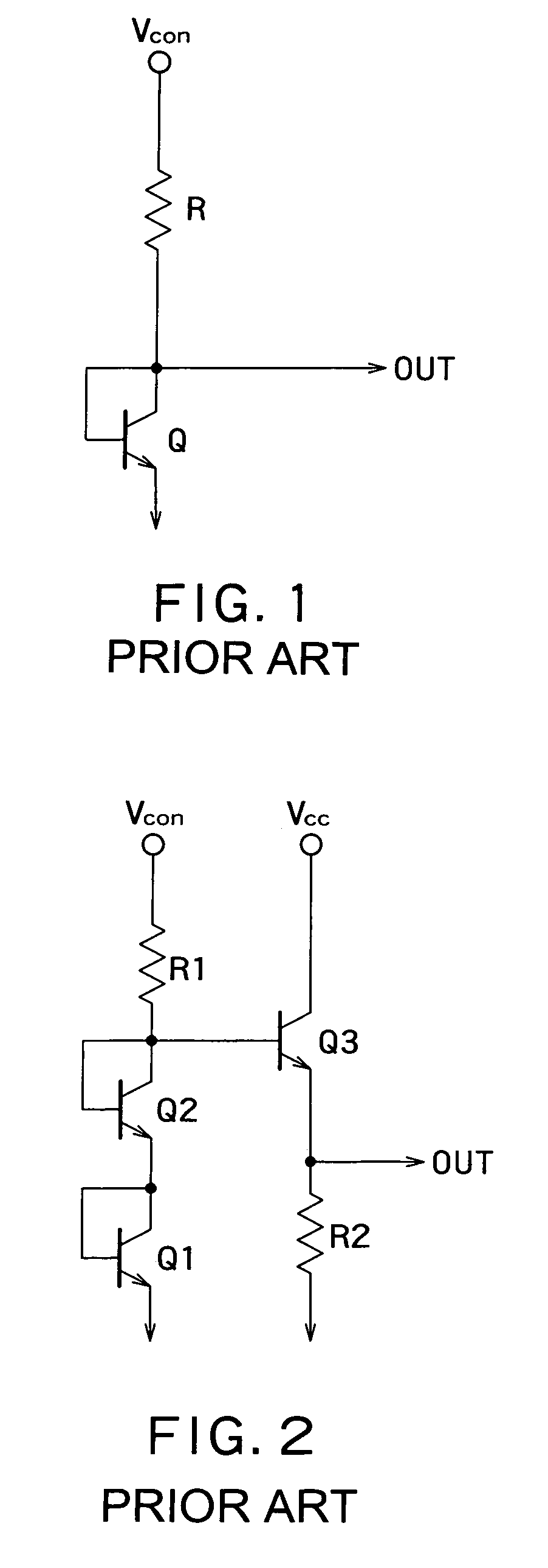
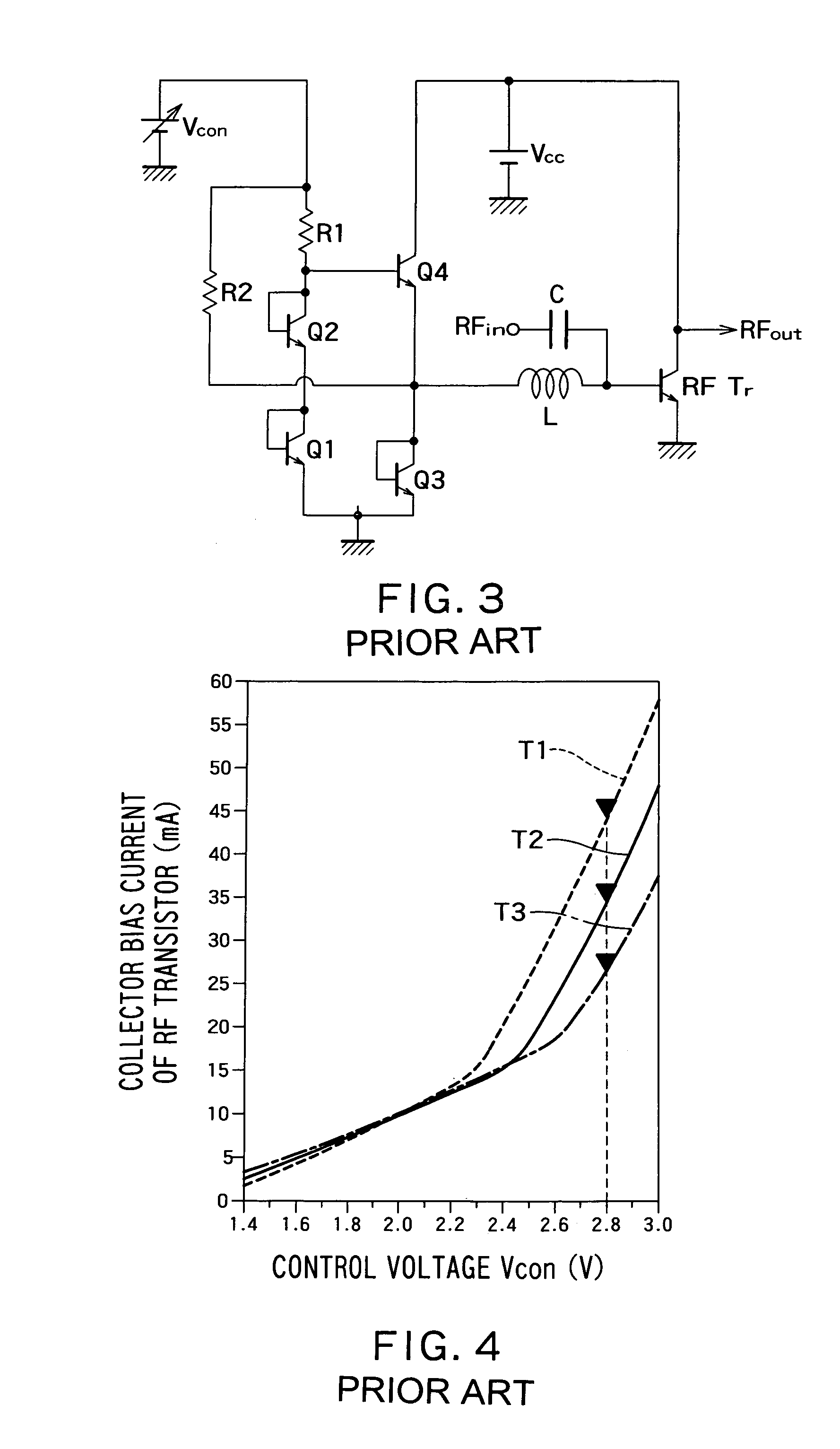
a current supply circuit and bias current technology, applied in the direction of amplifiers with impedence circuits, amplifiers with semiconductor devices only, amplifiers with discharge tubes, etc., can solve the problems of insufficient current supply, inability to maintain compensation for bias current fluctuation to temperature, and fluctuation in idle current, etc., to increase the amount of current supply, increase the base bias current, increase the effect of temperatur

Inactive Publication Date: 2006-03-07
KK TOSHIBA
View PDF3 Cites 25 Cited by
  • Summary
  • Abstract
  • Description
  • Claims
  • Application Information

AI Technical Summary

Benefits of technology

[0049]a bias current compensation circuit which has the normal temperature characteristics increasing the amount of current supply with increasing temperature and suppresses an increase in the base bias current with increasing ambient temperature by supplying a base current to the second bipolar transistor to pass a part of the base bias current supplied from an emitter of the first bipolar transistor through the second bipolar transistor.

Problems solved by technology

However, in the current mirror circuit including the diode-connected bipolar transistor shown in FIG. 1, the sufficient current can not be supplied.
However, since the conventional current mirror type base bias current supply circuit shown in FIG. 2 has the configuration in which the bipolar transistors are connected in two-stage series, unless the control voltage Vcon is sufficiently increased more than double voltage of on-voltage Vbeon of the transistor, it is impossible to maintain compensation for a fluctuation in bias current to temperature change, in which responsiveness is required.
However, in a system such as a cellular phone in which the control voltage is low, that the control voltage Vcon is increased is contrary to a flow of technical advance, so that there is generated a problem.
Particularly, in the system in which linear operation is required in the wide output dynamic range like a CDMA communication system, a fluctuation in idle current caused by the temperature change, which is largely affected during low output, becomes the problem.

Method used


Image

  • Bias current supply circuit and amplification circuit
  • Bias current supply circuit and amplification circuit
  • Bias current supply circuit and amplification circuit

Examples


first embodiment

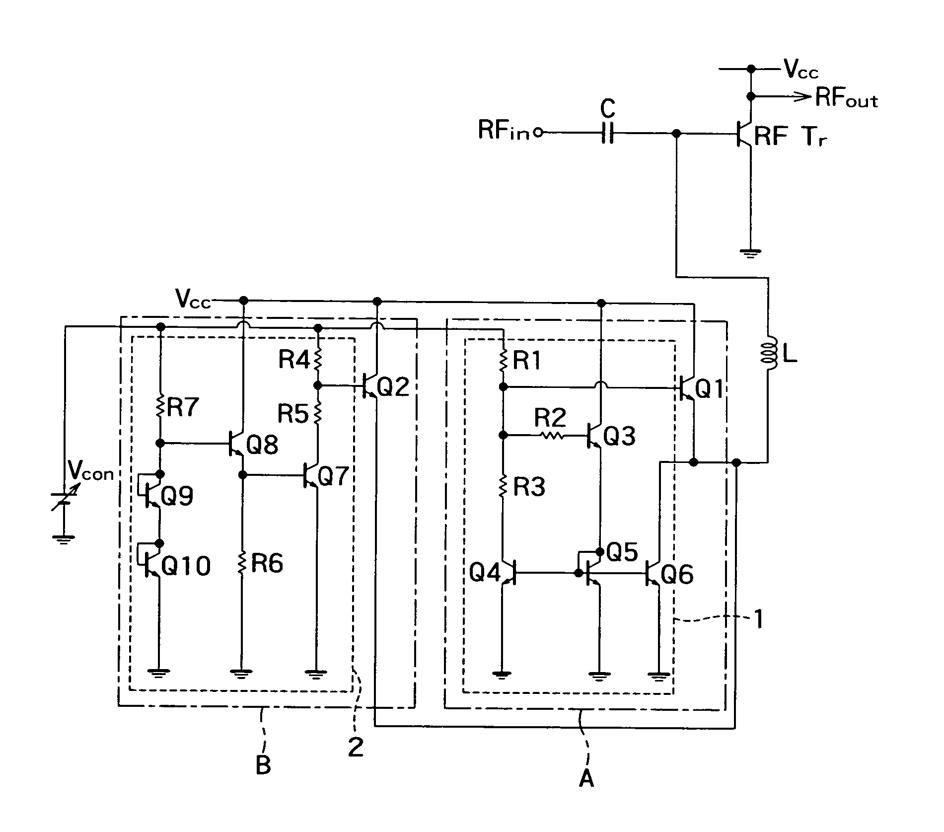
[0140]FIG. 5 is the circuit diagram showing a basic configuration of the bias current supply circuit and the amplification circuit according to the invention.

[0141]The bias current supply circuit according to the first embodiment of the invention includes a first bipolar transistor Q1 and a resistor R which are sequentially connected in series between the power supply potential node to which the power supply voltage Vcc is supplied and the ground potential node, a second bipolar transistor Q2 which is connected in parallel with the first bipolar transistor Q1, a normal temperature characteristic circuit 1 which has normal temperature characteristics increasing an amount of current supply with increasing temperature and is operated by supply of the control voltage Vcon to control the base current supplied to the first bipolar transistor Q1, and a reverse temperature characteristic circuit 2 which has reverse temperature characteristics decreasing the amount of current supply with inc...

second embodiment

[0174]FIG. 9 is the circuit diagram showing the basic configuration of the bias current supply circuit and the amplification circuit according to the invention.

[0175]The bias current supply circuit according to the second embodiment of the invention includes a first bipolar transistors Q1 and a second bipolar transistor Q2 which are sequentially connected in series between the power supply potential node to which the power supply voltage Vcc is supplied and the ground potential node, a normal temperature characteristic circuit 1 which has the normal temperature characteristics increasing the amount of current supply with increasing temperature and is operated by the supply of the control voltage Vcon to control the base current supplied to the first bipolar transistor Q1, and a bias current compensation circuit 3 which has the normal temperature characteristics increasing the amount of current supply with increasing temperature and controls the bias current supplied from the emitter...

third embodiment

[0209]FIG. 12 is the circuit diagram showing the configuration of the bias current supply circuit and the amplification circuit according to the invention.

[0210]The bias current supply circuit according to the third embodiment of the invention includes a resistor R1 and a bipolar transistor Q1 which are sequentially connected in series between the control potential node to which the control voltage Vcon is supplied and the ground potential node, a bipolar transistor Q2 in which the collector is connected to the power supply potential node to which the power supply voltage Vcc is supplied, the base is connected to the collector of the transistor Q1, and the emitter is connected to the base of the transistor Q1, a resistor R3 which is connected between the emitter of the transistor Q2 and the ground potential node, a bipolar transistor Q4 in which the collector is connected to the power supply potential node and the base is commonly connected to the base of the transistor Q1, a diode-...


PUM


Abstract

A bias current supply circuit according to an embodiment of the invention includes a first transistor and a second transistor which form two emitter followers cooperating to supply a base bias current of a bipolar transistor for signal amplification, a normal temperature characteristic circuit which has normal temperature characteristics increasing an amount of current supply with increasing temperature and supplies a base current to the first bipolar transistor, and a reverse temperature characteristic circuit which has reverse temperature characteristics decreasing the amount of current supply with increasing temperature and supplies a base current to the second bipolar transistor.

Description

CROSS REFERENCE TO RELATED APPLICATION[0001]The subject application is related to subject matter disclosed in Japanese Patent Application No. 2003-066733 filed on Mar. 12, 2003 in Japan to which the subject application claims priority under Paris Convention and which is incorporated herein by reference.BACKGROUND OF THE INVENTION[0002]1. Field of the Invention[0003]The present invention relates to a bias current supply circuit and an amplification circuit including the bias current supply circuit. Particularly the invention relates to the high-efficiency, high-power amplification circuit which is configured to use a bipolar transistor and operated by low power-supply voltage, and the bias current supply circuit which is added to the amplification circuit.[0004]2. Related Background Art[0005]In the high-efficiency, high-power amplification circuit which is configured to use the bipolar transistor and operated by the low power-supply voltage, since a collector current is greatly influ...

Claims


Application Information

Patent Timeline
Patent Type & Authority Patents(United States)
IPC IPC(8): H03F3/04H03F1/02H03F1/30H03F3/19H03F3/50
CPCH03F1/0261H03F3/50H03F3/19H03F1/302
Inventor KURIYAMA, YASUHIKO
Owner KK TOSHIBA
Why Eureka
Try Eureka