Single ku-band multi-polarization gallium arsenide transmit chip

a transmit chip and gallium arsenide technology, applied in the field of multipolarization active array transmit antennas, can solve the problems of transmit tileTM also displaying a higher level of spurious noise, unsatisfactory thick array, etc., and achieve low cost, low axial ratio, and thinning transmit phased array antennas.

Inactive Publication Date: 2006-03-07
HARRIS CORP
View PDF5 Cites 46 Cited by
  • Summary
  • Abstract
  • Description
  • Claims
  • Application Information

AI Technical Summary

Benefits of technology

[0019]According to another aspect of the present invention, the transmitter chip can be used to create a thinner transmit phased array antenna.
[0020]According to yet another aspect of the present invention, the transmitter chip

Problems solved by technology

The structure of a Transmit Tile™ containing five substrates makes it an undesirably thick array.
A Transmit Tile™ also displays a higher level of spurious noise due to signal leakage and coupling between channels of the circula

Method used


Image

  • Single ku-band multi-polarization gallium arsenide transmit chip
  • Single ku-band multi-polarization gallium arsenide transmit chip
  • Single ku-band multi-polarization gallium arsenide transmit chip

Examples


Embodiment Construction

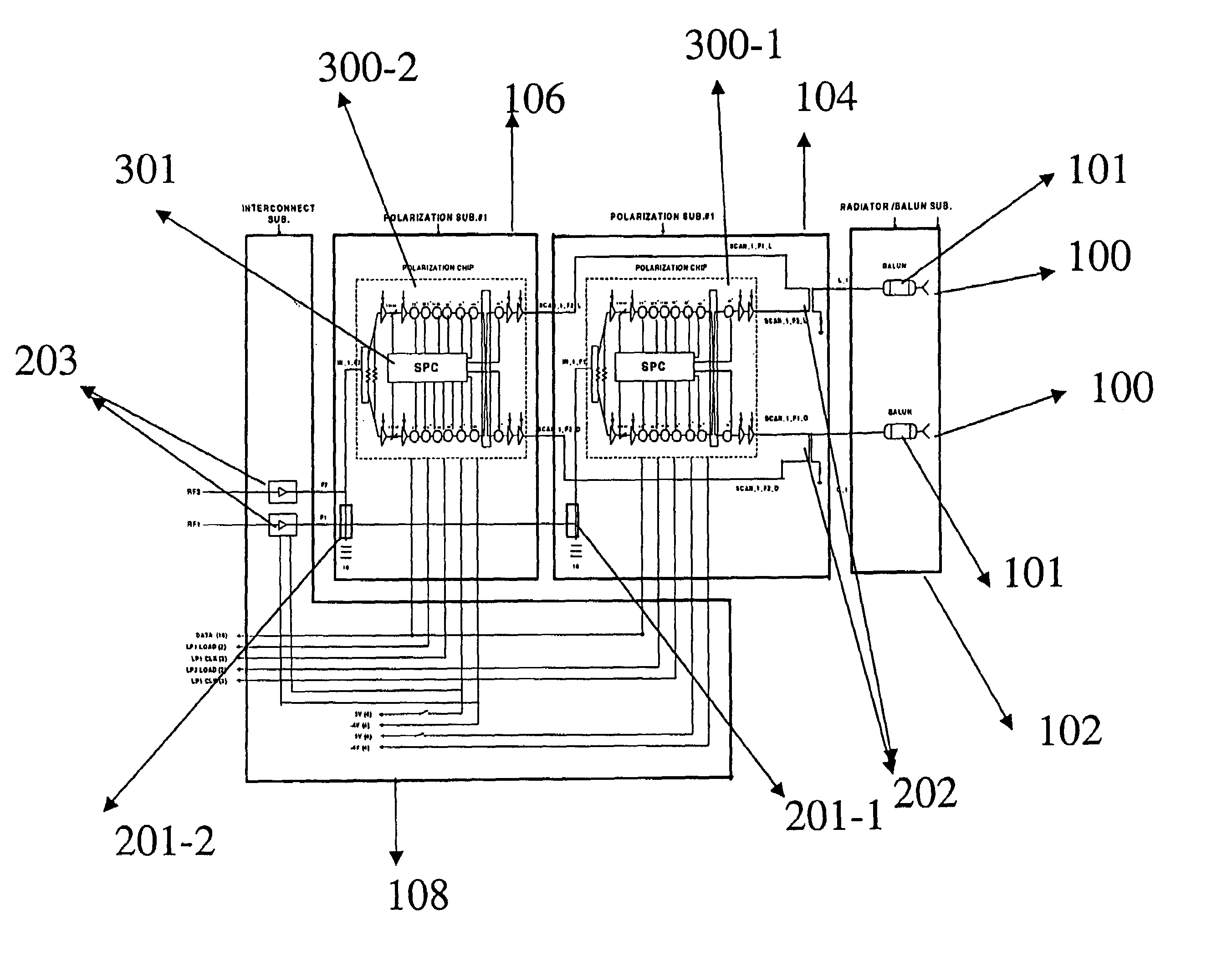
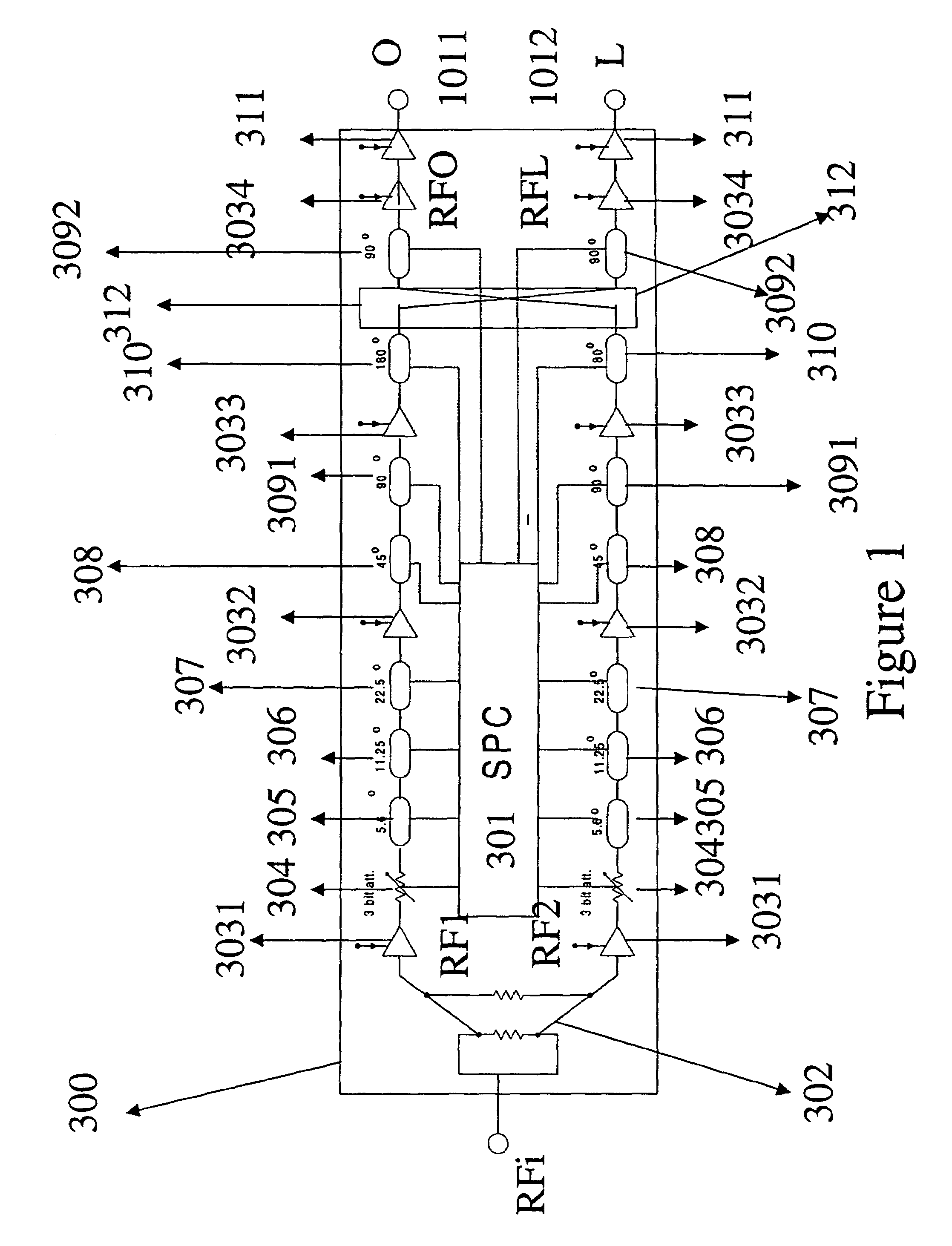
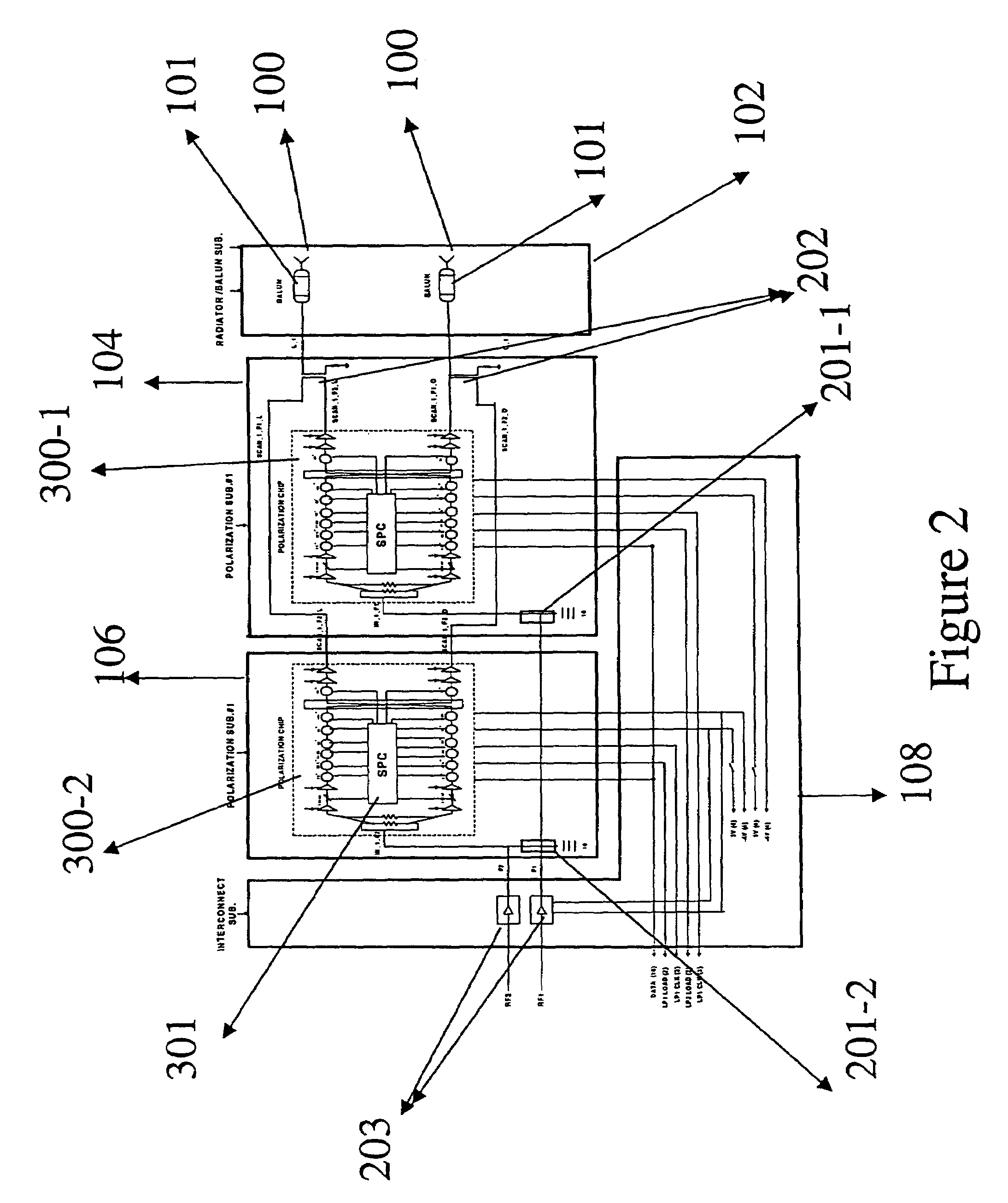
[0033]FIG. 1 is a functional block diagram of a transmitter chip 300 according to an embodiment of the present invention. According to this embodiment, the input signal RFi is connected to a two-stage divider 302. The outputs RF1 and RF2 from the divider 302 are input into two single-stage amplifiers 3031. The output signals from each single stage amplifier 3031 is input into a 3-bit attenuator 304. The output from each of the 3-bit attenuators 304 is input into a 5.625° phase shifter 305. The output from each of the 5.625° phase shifters 305 is input into a 11.25° phase shifters 306. The output from each of the 11.25° phase shifters 306 is input into a 22.5° phase shifter 307. The output from each of the 22.5° phase shifter 307 is input into a single-stage amplifier 3032. The output from each of the single-stage amplifiers 3032 is input into a 45° phase shifter 308. The output from each of the 45° phase shifter 308 is input into a 90° phase shifters 3091. The output from each of th...


PUM


Abstract

The present invention is a wide band GaAs microwave monolithic integrated circuit (MMIC) transmit chip that is capable of transmitting linearly or circularly polarized signals when connected to a pair of orthogonal cross-polarized antennas. In an active phased-array antenna environment, this transmit chip is capable of transmitting signals with different scan angles. This invention also contains a digital serial to parallel converter that uses TTL signal to control the phase shifter and attenuator circuits that are required for controlling the polarization and scan angle of the transmitted signal.

Description

RELATED APPLICATIONS[0001]This application is a divisional of pending U.S. application Ser. No. 10 / 014,553 filed on 14 Dec. 2001.FIELD OF THE INVENTION[0002]The present invention generally relates to a multi-polarization active array transmit antenna.BACKGROUND OF THE INVENTION[0003]Array transmit antenna technology is widely used in the area of satellite telecommunication, data transmission, radar systems and voice communication systems. Array antennas use electronic scanning technologies, such as time delay scanning, frequency scanning, or phase scanning to steer the transmitted beam. Use of electronic scanning allows an antenna system to achieve increased transmission data rates, instantaneous beam positioning, and the ability to operate in a multi-target mode. By using electronic scanning technology, an array transmit antenna can perform multiple functions that are otherwise performed by several separate antenna systems. Of the several electronic scanning technologies, phase sca...

Claims


Application Information

Patent Timeline
IPC IPC(8): H01Q1/38G01S13/00H01Q21/00
CPCH01Q21/0025
Inventor JENABI, MASUD
Owner HARRIS CORP
Why Eureka
Try Eureka