Three-dimensional measurement device and three-dimensional measurement method

Inactive Publication Date: 2006-03-07
MINOLTA CO LTD
View PDF10 Cites 34 Cited by
  • Summary
  • Abstract
  • Description
  • Claims
  • Application Information

AI Technical Summary

Benefits of technology

[0010]An object of the present invention is to eliminate the previously described disadvantages. Another object of the present invention is to realize high-resolution three-dimensional measurement in a compact form factor. Another object of the pres

Problems solved by technology

It is difficult to make a device compact since a light modulation device must be included in a construction for controlling the exposure timing of the solid state area sensor by light modulation as described above.
In a construction for standardizing the amount of light of the reflected pulse light, disadvantages arise inasmuch as the allowed range of reflectivity of the object and the m

Method used


Image

  • Three-dimensional measurement device and three-dimensional measurement method
  • Three-dimensional measurement device and three-dimensional measurement method
  • Three-dimensional measurement device and three-dimensional measurement method

Examples


Example

First Embodiment

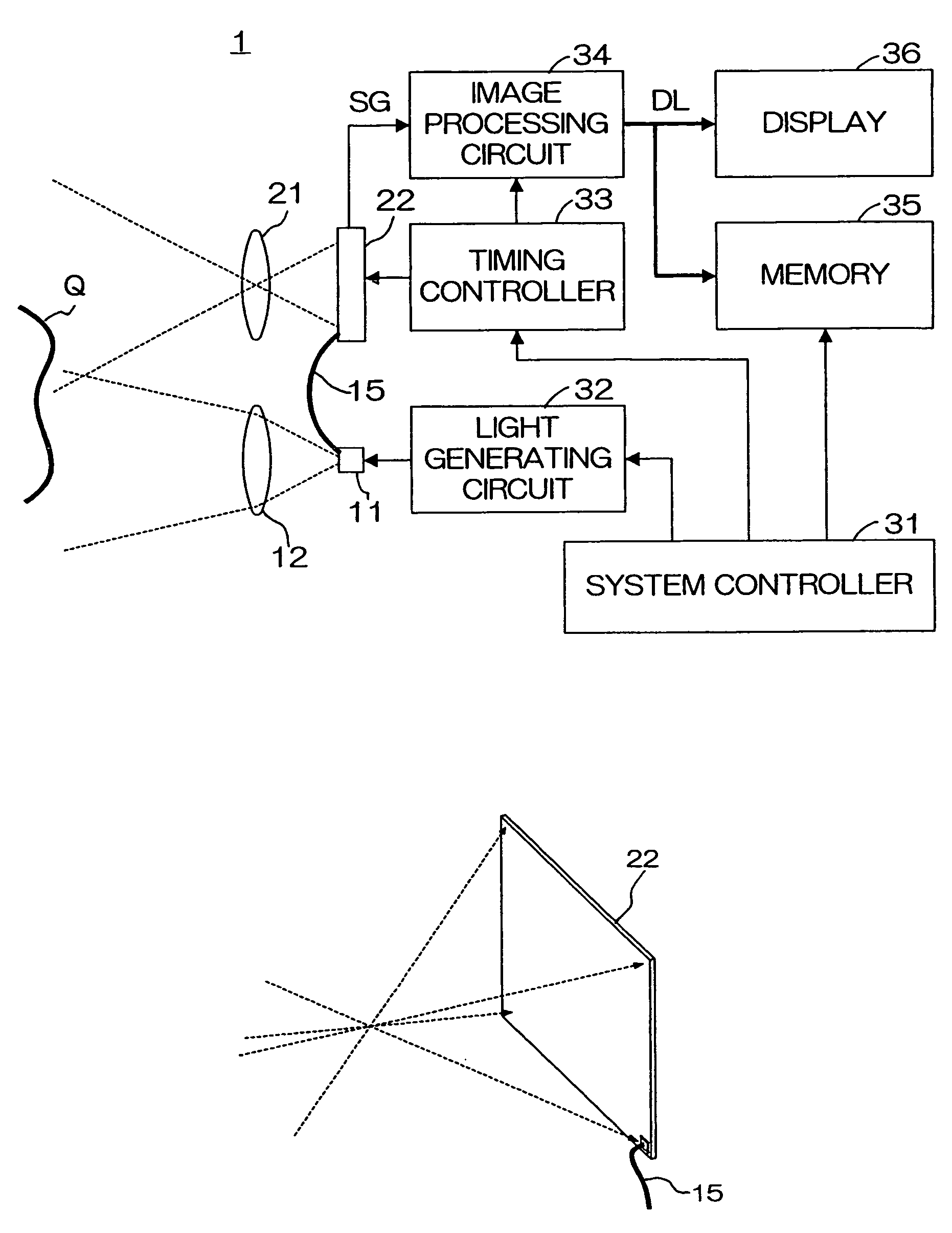
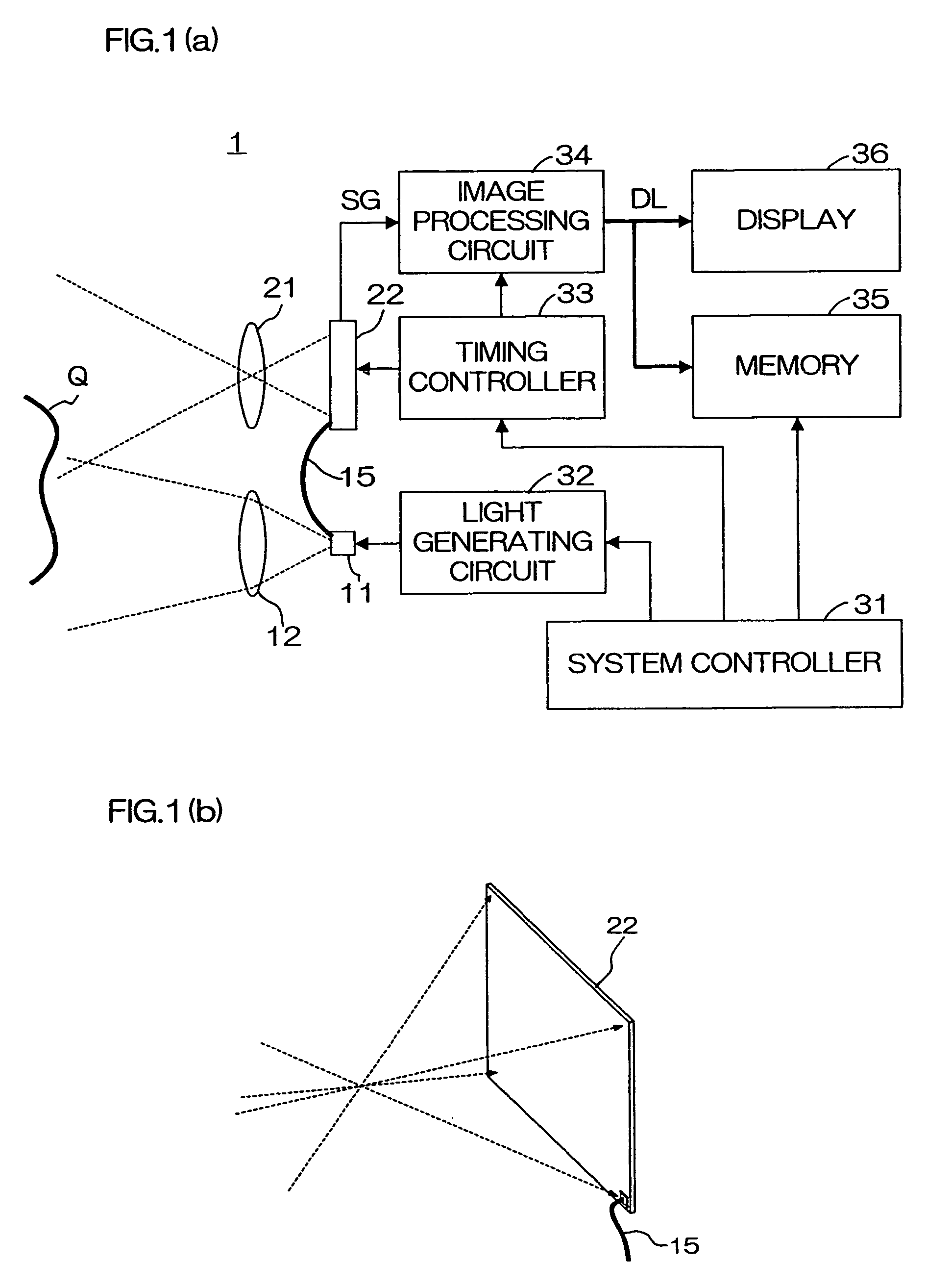
[0035]Device Structure

[0036]FIGS. 1(a) and 1(b) show the structure of a three-dimensional measure device of the first embodiment. FIG. 1(a) shows the entire structure, and FIG. 1(b) shows the structure of the image sensing surface.

[0037]A three-dimensional measurement device 1 is provided with a light source 11, projection lens 12, light receiving lens 21, and solid state area sensor 22. The light source 11 receives power from a light generating circuit 32, and emits laser light. An object Q is illuminated by the laser light passing through the projection lens 12. The light reflected from the object Q passes through the light receiving lens 21, and impinges the solid state area sensor 22. The solid state area sensor 22 has pixels which block the light from outside the device, and part of the laser light from the light source 11 passes through an internal optical path 15 comprised of optical fiber without passing outside and directly impinges the pixel as “standard li...

Example

Second Embodiment

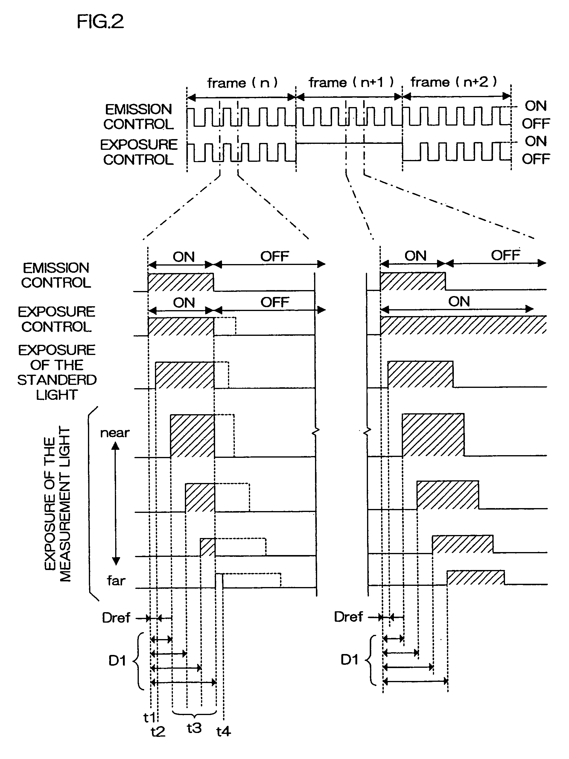
[0105]Laser light is most suitable as the signal medium in distance measurement using the TOF method. However, since measurement of light propagation time is an event performed at high speed, it is difficult to ensure high accuracy at near-field distances. measurement of constant precision can be realized regardless of whether the distance is near-field or not by using the TOF method and the triangulation method.

[0106]Device Construction

[0107]FIG. 18 shows the structure of a three-dimensional measurement device of the second embodiment.

[0108]The three-dimensional measurement device 2 has, in addition to the structural elements of the three-dimensional measurement device 1 shown in FIG. 1, a triangulation density gradient filter 19, filter controller 38, and mode switch 39.

[0109]The function of the density gradient filter 19 is variable, an includes projecting a first light and a second light having different luminous intensity distributions, and a substantially thro...


PUM


Abstract

The purpose of the present invention is to realize a compact three-dimensional measurement device of high resolution. In the present invention, a pulse light is projected on an object, the light reflected from the object is received by a solid state area sensor having a plurality of photoelectric conversion elements, the area sensor is controlled with a timing synchronized with the projection of the pulse light, and the distance to each photoelectric conversion element is measured based on the output of the solid state area sensor.

Description

RELATED APPLICATION[0001]This application is based on Patent Application No. 2000-155768 filed in Japan, the entire content of which is hereby incorporated by reference.BACKGROUND OF THE INVENTION[0002]1. Field of the Invention[0003]The present invention relates to a three-dimensional measurement method and device for obtaining position information of an object by projecting light and receiving the light reflected from the object.[0004]2. Description of the Related Art[0005]Three-dimensional measurement can be accomplished using the time of flight (TOF) from the moment of light pulse transmission to the reception of the returning light pulse reflected by an object since this TOF is dependent on distance.[0006]Japanese Laid-Open Patent Application No. H11-508371 discloses a device using a solid state area sensor as a photoreceptor device for modulating light entering the solid state area sensor by a photoelectric modulator. The distance is reflected in the amount of exposure light of...

Claims


Application Information

Patent Timeline
IPC IPC(8): G01C3/00G01C3/08G01C5/00G06K9/00G01B11/00G01B11/25G01C3/06G01S7/4863G01S7/4865G01S17/14G01S17/42G01S17/46G01S17/89G06F3/00G06F3/038G06F3/0487
CPCG01B11/25G01S7/4863G01S7/4865G06T7/0057G01S17/105G01S17/42G01S17/89G01S7/497G06T7/521G01S17/14
Inventor KAMON, KOICHINORITA, TOSHIOUCHINO, HIROSHI
Owner MINOLTA CO LTD
Why Eureka
Try Eureka