Method and system for cleaning a polishing pad

a technology of polishing pad and cleaning method, which is applied in the direction of grinding machine components, manufacturing tools, abrasive surface conditioning devices, etc., can solve the problems of step coverage, distorted pattern image, and inability to form the intended structure, so as to minimize the interruption of the polishing process and improve production throughput , the effect of jeopardizing the quality of the subsequent polishing process

Active Publication Date: 2006-03-21
MONTEREY RES LLC
View PDF7 Cites 18 Cited by
  • Summary
  • Abstract
  • Description
  • Claims
  • Application Information

AI Technical Summary

Benefits of technology

[0020]There may be several advantages to creating a method and system to remove the build-up of matter upon a polishing pad during a CMP process. For example, the fact that the system is incorporated into the CMP process may minimize interruption of the polishing process. Consequently, production throughput may be increased. In addition, the spray element included in such a system is preferably adapted to spray a fluid at a sufficient pressure such that essentially all of the matter is removed from the pad. In this manner, the pad may be cleansed completely before polishing one or more wafers. Conventional methods typically do not remove all of the matter on a pad, thereby jeopardizing the...

Problems solved by technology

For example, problems with step coverage may arise when a dielectric, conductive, or semiconductive material is deposited over a topological surface having elevationally raised and recessed regions.
If a topography is non-planar, the patterned image may be distorted and the intended structure may not be formed to the specifications of the device.
Furthermore, correctly patterning layers upon a topological surface containing fluctuations in elevation may be difficult using optical lithography.
The presence of such elevational disparities therefore makes it difficult to print high resolution features.
Unfortunately, the polishing rate performance of polishing systems and the resultant uniformity of wafers polished by such systems degrades as matter builds up in the pores and on the upper surface of the polishing pad during the polishing process.
Such clogging restricts the amount of slurry that is able to fill the pores and consequently limits the amount of slur...

Method used


Image

  • Method and system for cleaning a polishing pad
  • Method and system for cleaning a polishing pad
  • Method and system for cleaning a polishing pad

Examples


Embodiment Construction

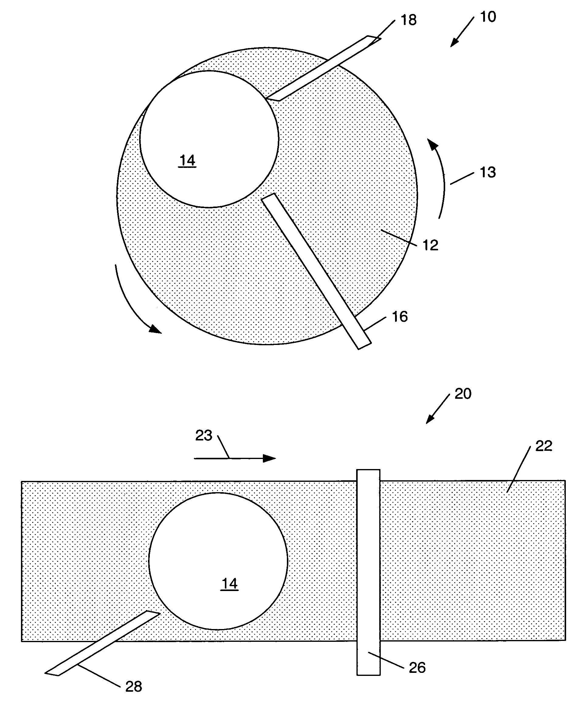
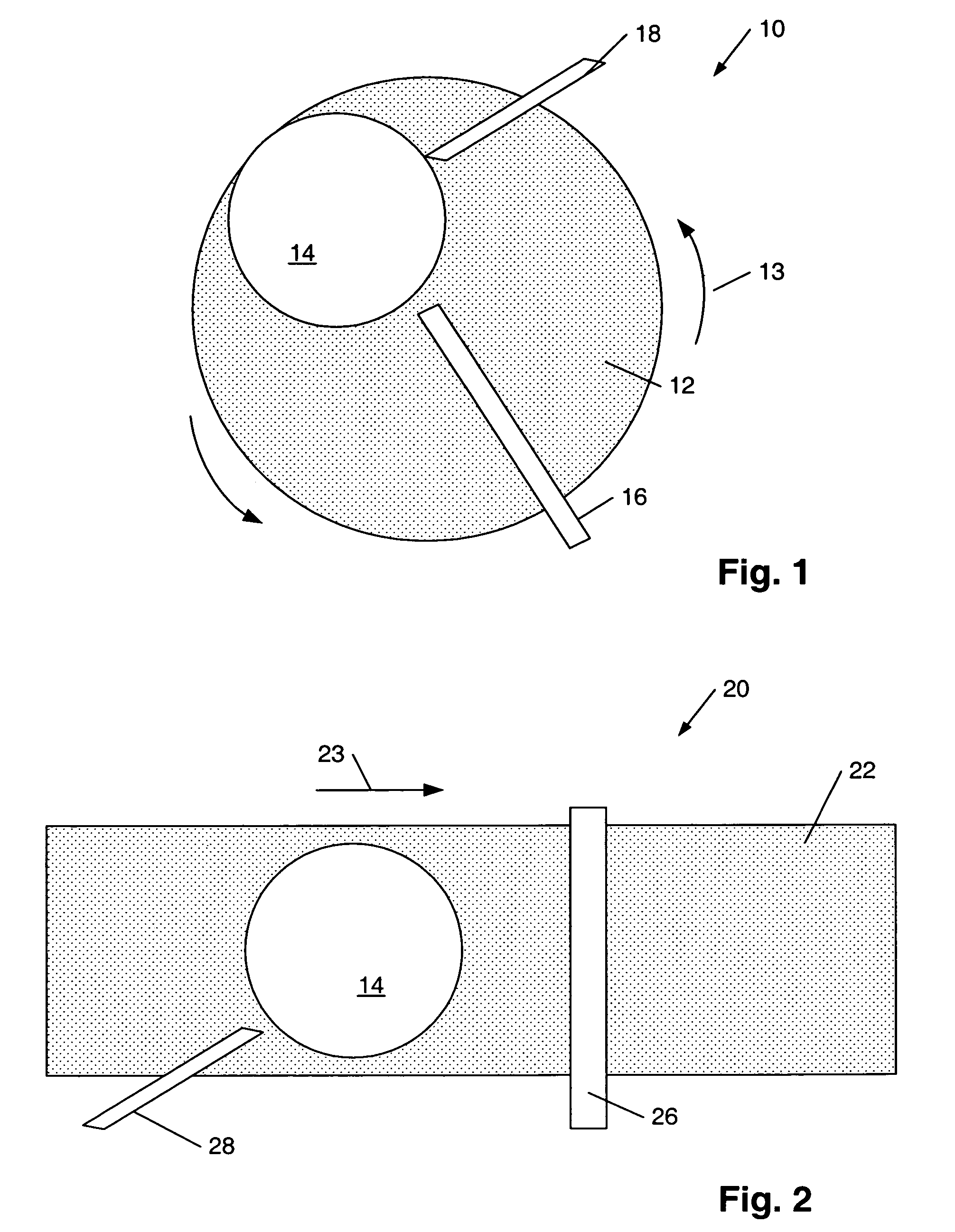
[0031]Turning to the drawings, an exemplary embodiment of a polishing system for processing a semiconductor topography according to the method as described herein is illustrated in FIG. 1. In particular, a partial top view of polishing system 10 is shown with polishing pad 12 positioned below semiconductor topography 14 and spray element 16. Polishing pad 12 may include a variety of materials depending on the process specifications of the fabrication process and / or design specifications of the subsequently formed semiconductor devices. In particular, materials used for polishing pad 12 may vary in hardness and surface texture depending on the design specifications of the polished topography and the process capabilities of the polishing system. For example, a CMP polishing system which has a polishing pad with an abrasive surface may have a higher ratio of mechanical polishing action versus chemical polishing. Moreover, a polishing system with a polishing pad that is particularly har...


PUM

PropertyMeasurementUnit
Pressureaaaaaaaaaa
Pressureaaaaaaaaaa
Pressureaaaaaaaaaa

Abstract

A method and a system are provided for removing matter adhered to such a polishing pad. In particular, a polishing system is provided which is adapted to remove matter adhered to a polishing pad during a polishing process of a semiconductor topography. The polishing system may include a polishing pad and a spray element, which is preferably adapted to spray a pressurized fluid upon the polishing pad to remove matter adhered to the pad. In addition, a spray element is provided which may be adapted to be positioned within a polishing system. Such a spray element may be adapted to remove matter adhered to a polishing pad within the system by spraying a pressurized fluid upon the polishing pad. In addition, methods for cleaning a polishing pad during a polishing process and polishing multiple semiconductor topographies using the systems described herein are provided.

Description

BACKGROUND OF THE INVENTION[0001]1. Field of the Invention[0002]This invention relates to semiconductor device manufacturing, and more particularly, to an improved method and system for removing matter adhered to a polishing pad.[0003]2. Description of the Related Art[0004]The following descriptions and examples are not admitted to be prior art by virtue of their inclusion within this section.[0005]Fabrication of an integrated circuit involves numerous processing steps. For example, after implant regions (e.g., source / drain regions) have been placed within a semiconductor substrate and gate areas defined upon the substrate, alternating levels of interlevel dielectric and interconnect may be placed across the semiconductor topography to form a multi-level integrated circuit. Such a multi-level integrated circuit may include a plurality of layers and structures. Forming substantially planar upper surfaces of the semiconductor topography during intermediate process steps of the process...

Claims


Application Information

Patent Timeline
IPC IPC(8): B24B1/00
CPCB24B53/017
Inventor COLLIER, RONALD E.ZAGREBELNY, ANDREY
Owner MONTEREY RES LLC
Why Eureka
Try Eureka