Circuit for performing on-die termination operation in semiconductor memory device and its method

a technology of semiconductor memory and circuit, which is applied in the direction of pulse technique, baseband system details, instruments, etc., can solve the problems of delay corresponding, the required specifications of the odt turn-on time taon and the odt turn-off time taof are not satisfied, and the excess of the odt turn-on time taon and the odt turn-off time taof over the required maximum specifications

Inactive Publication Date: 2006-03-28
SK HYNIX INC
View PDF2 Cites 44 Cited by
  • Summary
  • Abstract
  • Description
  • Claims
  • Application Information

AI Technical Summary

Benefits of technology

[0012]It is another object of the present invention to provide a circuit and its method which minimizes the effect of a delay on an ODT turn-on time tAON and an ODT turn-off time tAOF, the delay occurring due to architectures needed to a driving force of ODT associated control signals.
[0014]Preferably, the first flip-flop member further includes a member for increasing a driving force of the plurality of parallel output signals.
[0015]Preferably, the second flip-flop member further includes a member for increasing a driving force of the plurality of parallel output signals outputted from the first flip-flop member, prior to the control of the delayed lock loop clocks provided from the delayed locked loop.
[0020]Further, in accordance with the present invention, there is a method for performing an on-die termination (“ODT”) operation in a semiconductor memory device, which comprises the steps of: (a) outputting first and second buffered clocks using an external clock and an external inverting clock applied thereto externally; (b) comparing each other an on-die termination signal and a reference voltage, which are applied thereto from an external chip set, to generate an on-die termination comparison signal; (c) transferring the on-die termination comparison signal as a plurality of parallel output signals based on the first and second buffered clocks; (d) increasing a driving force of the plurality of parallel output signals; and (e) outputting the parallel output signals with an increased driving force based on delayed lock loop clocks outputted from a delayed lock loop.
[0022]In accordance with the present invention, it is capable of ensuring a time margin which satisfies specifications of an ODT turn-on time tAON and an ODT turn-off time tAOF, by removing two- or four-stage of inverters, which is needed to provide a driving force enough for allowing signals after the application of DLL clocks to be delivered to each pad.
[0023]Further, in accordance with the present invention, two- or four-stage of inverters are required between a first flip-flop member and a second flip-flop member in order to provide a driving force of signals outputted toward each pad. However, it is not affects on a maximum of the ODT turn-on time tAON and the ODT turn-off time tAOF. The reason for this is that the ODT turn-on time tAON and the ODT turn-off time tAOF are based on DLL clocks rclk_dll and fclk_dll provided from the second flip-flop member, and the two- or four-stage of inverters employed in the present invention is disposed at front of the second flip-flop member received the DLL clocks rclk_dll and fclk_dll. Therefore, the present invention is capable of increasing a time margin for a maximum specification of the ODT turn-on time tAON and the ODT turn-off time tAOF by the number of required stages of inverters.

Problems solved by technology

As a result, the prior art suffers from the disadvantage that there is likelihood of excess of the ODT turn-on time tAON and the ODT turn-off time tAOF over required maximum specifications.
Specifically, when the ODT enable signal ODT_enable is delivered to each pin according to the prior art, it suffers from the disadvantages that there is directly affected a distance deviation from the ODT enable signal generating member to each pin, and two- or four-stage of inverters are required for a driving force of the enable signal, in layout.
It results in a delay corresponding to the number of required inverter stages, and the required specifications of the ODT turn-on time tAON and the ODT turn-off time tAOF are not satisfied.

Method used


Image

  • Circuit for performing on-die termination operation in semiconductor memory device and its method
  • Circuit for performing on-die termination operation in semiconductor memory device and its method
  • Circuit for performing on-die termination operation in semiconductor memory device and its method

Examples


Embodiment Construction

[0034]Hereinafter, a semiconductor memory device in accordance with the present invention will be described in detail referring to the accompanying drawings.

[0035]While the present invention will be described more fully hereinafter with reference to the accompanying drawings, in which a preferred embodiment of the present invention is shown, it is to be understood at the outset of the description which follows that persons of skill in the appropriate arts may modify the invention here described while still achieving the favorable results of this invention. Accordingly, the description which follows is to be understood as being a broad, teaching disclosure directed to persons of skill in the appropriate arts, and not as limiting upon the present invention.

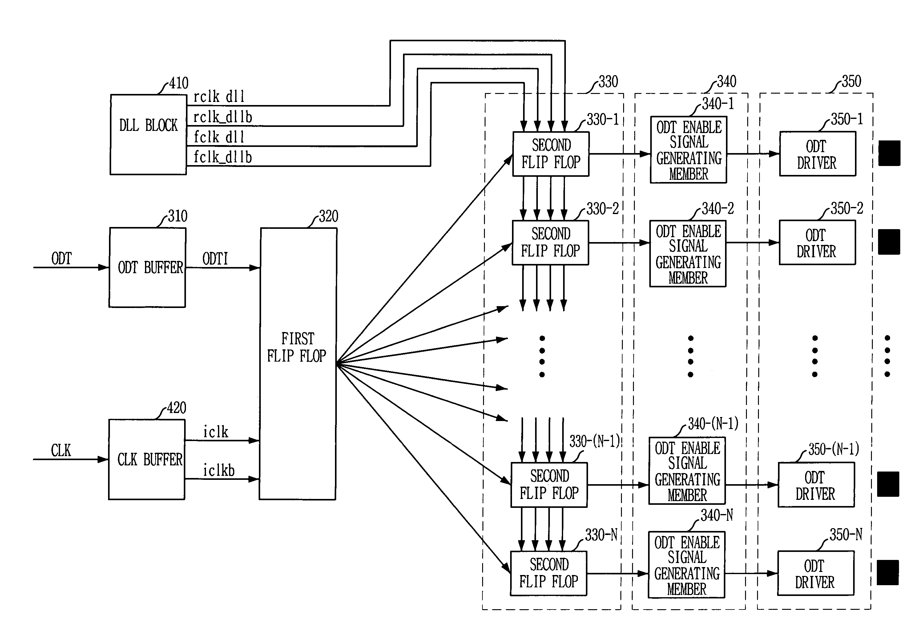
[0036]FIG. 3 is a block diagram of primary portions in a circuit in accordance with a preferred embodiment of the present invention, and FIG. 4 is an entire block diagram in the circuit in accordance with a preferred embodiment of t...


PUM


Abstract

A circuit for performing an on-die termination operation includes a clock buffer for outputting first and second buffered clocks using an external clock and an external inverting clock applied thereto externally; an on-die termination buffer for comparing each other an ODT signal and a reference voltage, which are applied thereto from an external chip set, to generate an on-die termination comparison signal; a first flip-flop member for transferring the on-die termination comparison signal as a plurality of parallel output signals based on the first and second buffered clocks outputted from the clock buffer; and a plurality of second flip-flop members, which corresponds to each of the parallel output signals outputted from the first flip-flop member, for transferring the parallel output signals outputted from the first flip-flop member based on delayed lock loop clocks outputted from a delayed lock loop.

Description

FIELD OF INVENTION[0001]The present invention relates to an On-Die Termination (“ODT”) technique in semiconductor memory device.DESCRIPTION OF PRIOR ART[0002]The ODT technique has been introduced to minimize a signal reflection in an interface between a system based on SSTL (Stub Series Termination Logic)_ and a memory storage device, thereby improving a signal integrity. In a conventional DDR-_ SDRAM, a termination voltage (VTT) and a termination resistor (RTT) provided by a motherboard is controlled by a memory controller through the use of the ODT technique, thereby allowing a termination to be provided at DRAM.[0003]First, the simple description will be directed to the termination.[0004]It is assumed that there are two ranks on a memory module. When a memory controller reads data from DRAM of a first rank Rank1, the memory controller applies an ODT signal of a high level state to DRAM of a second rank Rank2. In the occasion, the DRAM the second rank Rank2 forms a termination on ...

Claims


Application Information

Patent Timeline
Patent Type & Authority Patents(United States)
IPC IPC(8): H03K19/003H03K19/00G11C7/10H04L25/02
CPCG11C7/1051H04L25/0278G11C7/222G11C7/1057G11C7/10
Inventor LEE, SANG-HEE
Owner SK HYNIX INC
Why Eureka
Try Eureka