

Active inductors using bipolar silicon transistors
a bipolar silicon transistor and active inductors technology, applied in the field of active inductors, can solve the problems of limited quality factor (q), disclosed transceivers lack versatility, and previously proposed configurations that do not provide the desired unconditional multimode front end
- Summary
- Abstract
- Description
- Claims
- Application Information
AI Technical Summary
Benefits of technology
Problems solved by technology
Method used
Image

Examples
first embodiment
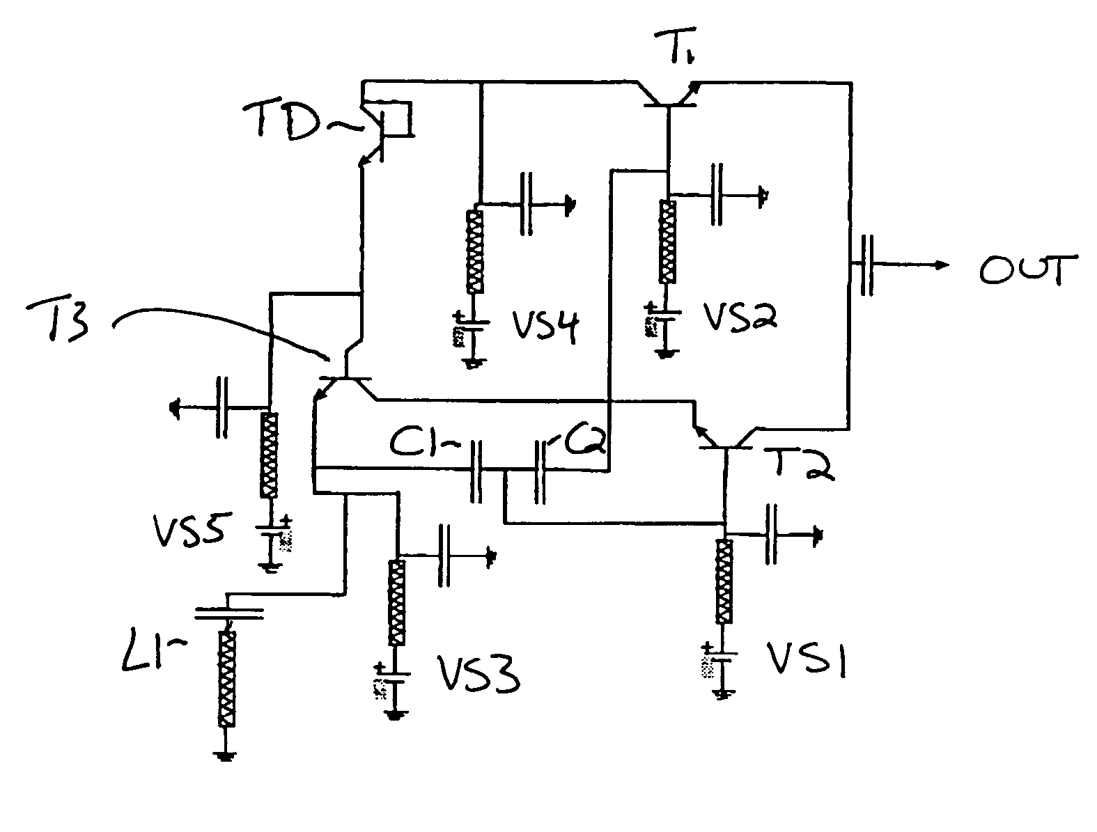
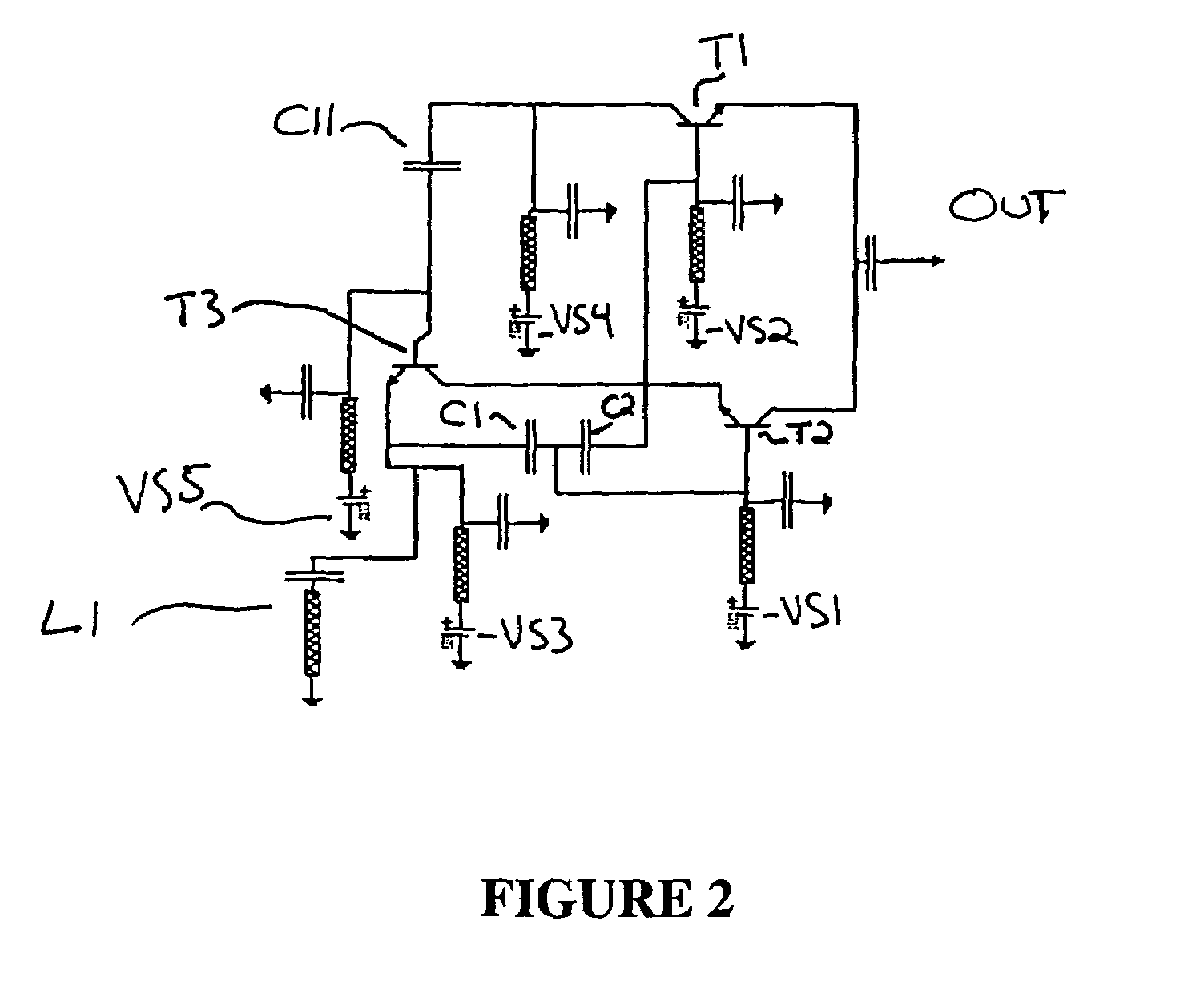
[0064]FIG. 3 depicts an active inductor according to the present invention. For simplicity, the same reference numbers are used to identify similar elements. The active inductor illustrated in FIG. 3 includes four transistors T1, T2, T3, and TD, which are connected as follows.
[0065]An emitter of a first transistor T1 is connected to an output port Vout and to a collector of a second transistor T2. A base of the second transistor T2 is connected to a voltage supply VS 1 and between a first and a second capacitor C1 and C2, which are connected together.
[0066]An emitter of the second transistor T2 is connected to a collector of a third transistor T3.
[0067]An end of the second capacitor C2, which is not connected to the base of the second transistor T2, is connected to a base of the first transistor T1 and to a voltage supply VS2. An end of the first capacitor C1, which is not connected to the second transistor T2, is connected to an emitter of T3, to a voltage supply VS3, and to a load...
embodiment 1
[0071]Optimization of the active inductor of embodiment 1 of the present invention requires adjustment of the voltages VS1–VS5. Preferably, VS2 and VS4 are adjusted to reduce the equivalent resistance Req. Preferably, VS3 and VS5 are adjusted to shift the optimal frequency. More preferably, the optimal frequency is achieved by simultaneously adjusting VS2 and VS4, provided that VS1, VS3, and VS5 are adjusted to match the biasing points of the four transistors T1–T3 and TD.
[0072]The active inductors of the present invention are not limited to any specific applications and practitioners will readily recognize that the active inductors can be used wherever a passive inductor is used. However, exemplary applications are provided to demonstrate the use of the active inductors in oscillators, amplifiers, and transceivers.
[0073]In actual communications systems, the use of oscillators to stabilize the working frequency is essential. A central component of most oscillators is an RLC circuit....
second embodiment
[0074]the present invention provides an adaptive oscillator, one example of which is illustrated in FIG. 6. The oscillator shown in FIG. 6 includes an HF amplifier with an accorded load, in which part of the output signal is re-injected in the input of the oscillator with the correct phase due to the correct transformation of a secondary self. The inductor Lactive is an active inductor of the present invention. In the exemplary oscillator depicted in FIG. 6, the capacitor Cosc suppresses the biasing perturbation from the output (provided that the impedance at the working frequency is negligible). The desired frequency is determined via the filtering effect of the LC factor. Namely, the active inductor Lactive acts in parallel with the capacitor Cosc to provide a filtering effect at a certain frequency with a high quality factor, thereby achieving a pure signal. Further, because the active inductor Lactive is a variable inductor, a direct means for optimizing the frequency is provide...
PUM
 Abstract
Description
Claims
Application Information