Methods and apparatus for laser marking of integrated circuit faults

a technology of integrated circuits and laser marking, which is applied in the field of integrated circuit failure analysis, can solve the problems of labor-intensive manual marking procedures, high labor intensity, and high labor intensity of manual marking procedures, and achieve the effect of increasing marking accuracy and throughpu

Inactive Publication Date: 2006-03-28
ALTERA CORP
View PDF7 Cites 28 Cited by
  • Summary
  • Abstract
  • Description
  • Claims
  • Application Information

AI Technical Summary

Benefits of technology

[0006]In accordance with the present invention, systems and methods are provided for marking integrated circuit faults for failure analysis. The systems and methods of the invention increase marking accuracy and throughput.

Problems solved by technology

Faults are often detected when debugging new integrated circuit designs.
This is generally accomplished using labor-intensive manual marking procedures.
Conventional marking arrangements such as these are labor intensive and prone to error.
It may take hours to mark a single wafer, particularly when the defects are hard to locate in the CAD file or when many manual alignments are required at the probe station.
Moreover, the process is dependent on the skills of the technician, which makes it difficult to control the accuracy of the process.

Method used


Image

  • Methods and apparatus for laser marking of integrated circuit faults
  • Methods and apparatus for laser marking of integrated circuit faults
  • Methods and apparatus for laser marking of integrated circuit faults

Examples


Embodiment Construction

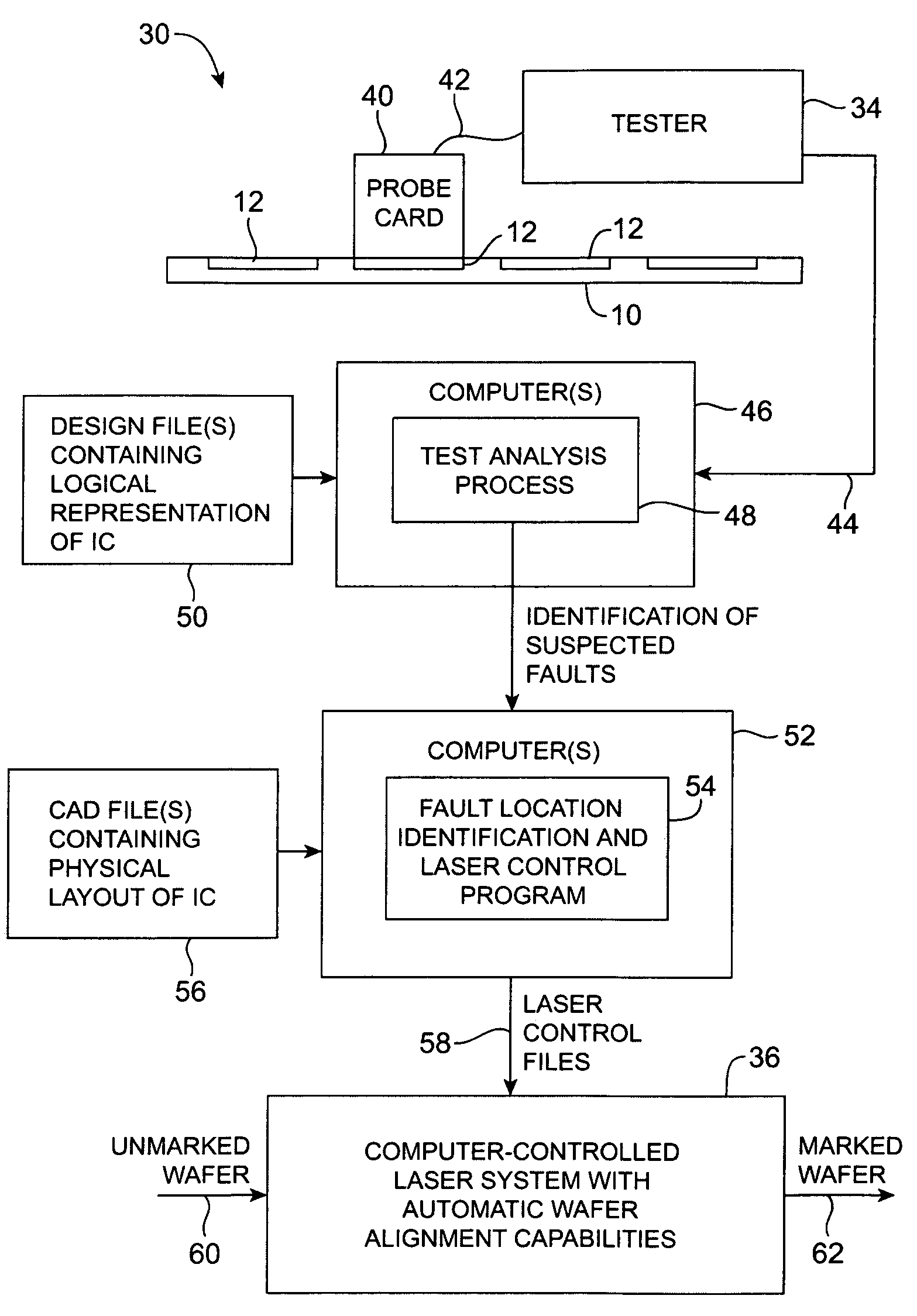
[0016]The present invention relates to systems and methods for marking faults on wafers of integrated circuits for failure analysis. After an integrated circuit has been designed, it is customary to fabricate a batch of test wafers. Each wafer typically contains numerous integrated circuits. In a production run, the wafers are diced into individual integrated circuit die and are packaged as individual circuits. However, during preliminary testing, the integrated circuits are not generally packaged. Rather, integrated circuits are subjected to electrical testing while they are still part of a test wafer.

[0017]The electrical testing process may reveal one or more faults (defects) on a wafer. For example, on a wafer of 13 integrated circuits, it may be determined that integrated circuit number five has an electrical fault in the second row and third column of a particular block of memory cells. With the present invention, physical position information may be automatically created for f...


PUM


Abstract

Systems and methods are provided for marking integrated circuit defects on wafers to facilitate failure analysis. A wafer containing integrated circuits can be tested using a tester. Test data from the tester can be analyzed using integrated circuit design files to identify suspected faults. A fault location program can be used to identify the physical location of the faults. The fault location program uses information on the faults identified and CAD file information on the physical layout of the integrated circuit to map identified faults to actual physical positions. The fault location program may also generate laser control files. The laser control files can be used to control a laser system so that the laser system creates laser marks on the wafer surrounding each of the faults. The marked faults can be polished and examined under an electron microscope or analyzed using other failure analysis tools.

Description

BACKGROUND OF THE INVENTION[0001]This invention relates to integrated circuit failure analysis, and more particularly, to methods and apparatus for marking faults on semiconductor wafers with lasers to facilitate failure analysis.[0002]Faults are often detected when debugging new integrated circuit designs. Typically, electrical testing is performed on a wafer of integrated circuits to identify faults. To investigate the nature of a suspected fault once it has been identified, it is often desirable to cleave and polish a piece of the wafer in the vicinity of the fault. The piece of polished wafer can then be examined under a scanning electron microscope. Analyzing manufacturing faults in this way allows the sources of faults to be eliminated during manufacturing.[0003]The locations of faults on a wafer must be precisely marked before cleaving and polishing. This is generally accomplished using labor-intensive manual marking procedures. With one known approach, a technician consults ...

Claims


Application Information

Patent Timeline
Patent Type & Authority Patents(United States)
IPC IPC(8): G06F11/30G01R31/28
CPCG01R31/2894G01R31/2831
Inventor DICOSOLA, JOHN M.WRIGHT, ADAMLEI, JUNZHAO J.BANKE, MARK A.HATA, WILLIAM
Owner ALTERA CORP
Why Eureka
Try Eureka