Microprocessor

Inactive Publication Date: 2006-03-28
PANASONIC CORP
View PDF8 Cites 12 Cited by
  • Summary
  • Abstract
  • Description
  • Claims
  • Application Information

AI Technical Summary

Benefits of technology

[0010]In view of the above-mentioned problem, an object of the present invention is to provide a microprocessor with a mechanism that is capable of reducing electric power consumption in execution of data calculation, while maintaining the level of calculation performance required for different types of data that are treated in different application programs to be executed by the microprocessor.
[0011]Another object of the present invention is to provide a microprocessor that is capable of increasing the speed of data calculation when application programs to be executed treat a certain type of data that satisfies a condition. Since microprocessors are required to be all-purpose and to work on various kinds of data, such capability is beyond a basic performance level of microprocessors.

Problems solved by technology

Since microprocessors are required to be all-purpose and to work on various kinds of data, such capability is beyond a basic performance level of microprocessors.

Method used


Image

  • Microprocessor
  • Microprocessor
  • Microprocessor

Examples


first embodiment

1. First Embodiment

[0053]The following describes the processor 100 in the first embodiment of the present invention, with reference to FIGS. 1 through 5.

1-1. General Structure

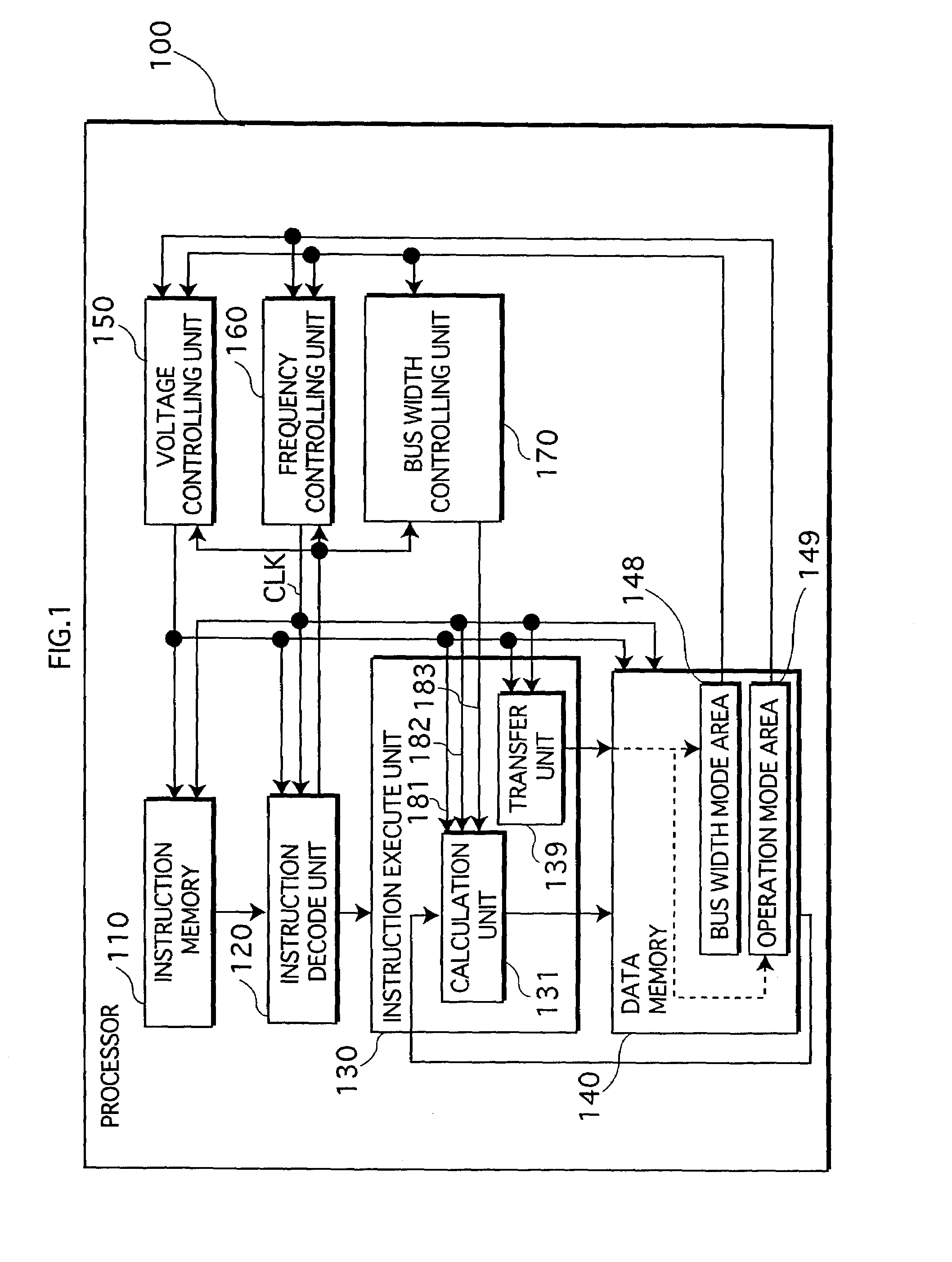
[0054]FIG. 1 is a functional block diagram of the processor 100 in the first embodiment of the present invention.

[0055]The processor 100 is a processor that decodes instructions in a program stored in an external memory and executes processing specified by those instructions. The processor 100 is constructed with a CMOS (Complementary Metal Oxide Semiconductor) and includes the instruction memory 110, the instruction decode unit 120, the instruction execute unit 130, the data memory 140, the voltage controlling unit 150, the frequency controlling unit 160, and the bus width controlling unit 170, as shown in the functional block diagram in FIG. 1.

[0056]It should be noted here that the instruction memory 110 is a cache memory for storing instructions to be executed that are fetched from an external memory. The ex...

second embodiment

2. Second Embodiment

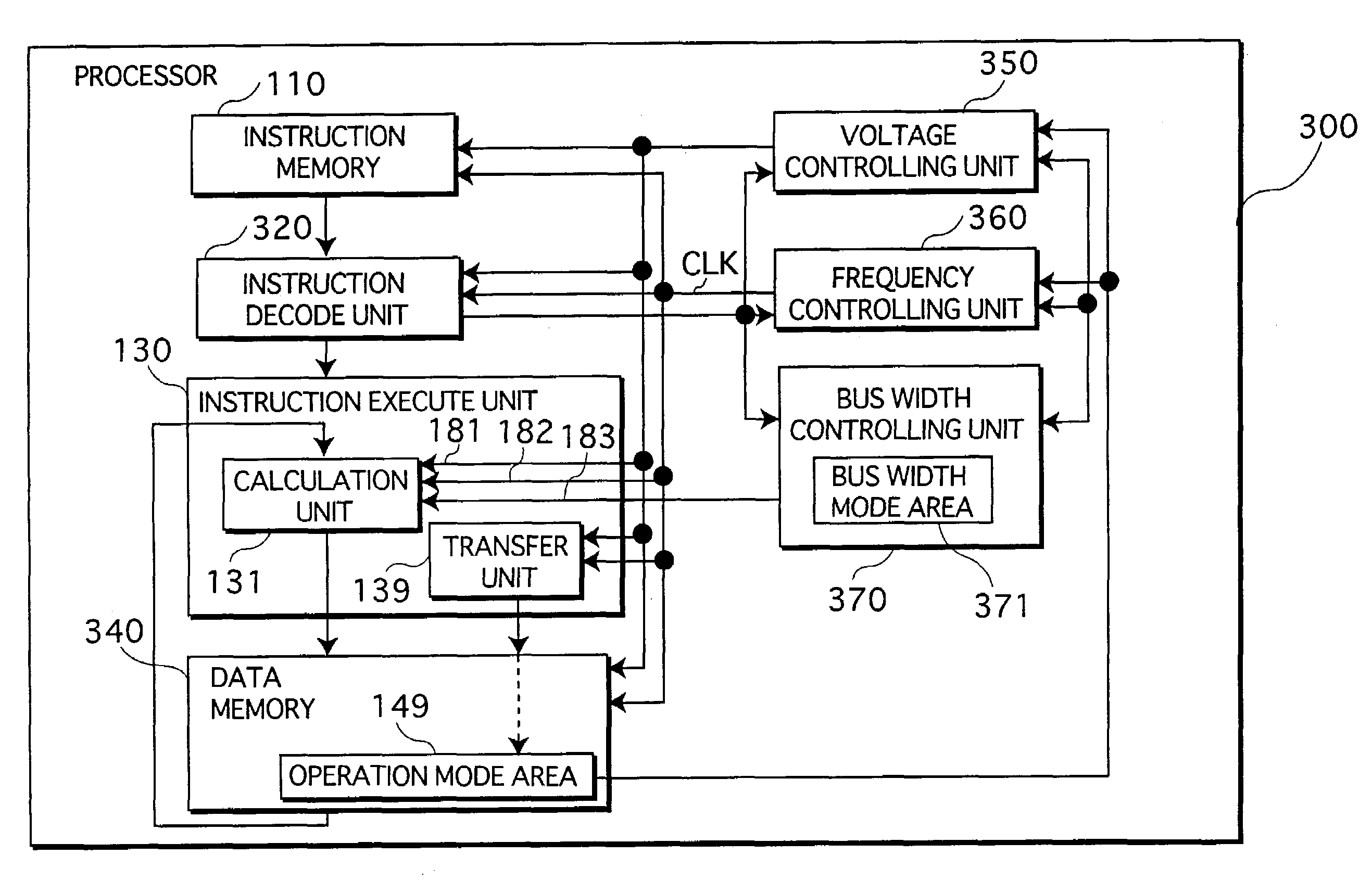
[0118]The following explains the processor 300 in the second embodiment, in which part of the processor 100 in the first embodiment is modified, with reference to FIGS. 6 and 7.

[0119]The processor 300 is different from the processor 100 in that the processor 300 changes the bus width mode individually for each instruction to be executed, depending on the number of bits in the data to be calculated under calculation instructions such as an add instruction in an application program, whereas the processor 100 was basically on an assumption that it changes the bus width mode for each application program to be executed.

[0120]FIG. 6 is a functional block diagram of the processor 300 in the second embodiment of the present invention. It should be noted that some of the components of the processor 300 which are virtually the same as the components of the processor 100 are indicated in FIG. 6 with same characters as in the FIG. 1, and detailed explanation of those same co...

third embodiment

3. Third Embodiment

[0135]The following explains a modification in which a special write control is performed for writing into a part of the data memory 140 a piece of 16-bit data (dest [15:0]) and a carry bit signal (carry) both outputted by the calculation unit 131 in the processor 100 in the first embodiment, with reference to FIG. 8.

[0136]FIG. 8 is a diagram to show a part of the data memory 140 that is capable of performing write control in the third embodiment.

[0137]The data storing areas 141a, 141b, and 141c are an area for 8 bits, 4 bits, and 4 bits respectively, and these three data storing areas together make a 16-bit register. Each of the data storing areas is independent, and is arranged so that only when it receives a write signal, it will store in a storage element the data on the buses, which is a result outputted by the calculation unit 131.

[0138]The write controlling unit 143 is a circuit that performs control for having the data outputted by the calculation unit 131...


PUM


Abstract

A microprocessor comprises a calculation unit that (i) includes partial calculation units each operable to perform partial data calculation, and (ii) is operable to perform data calculation on N or less bits, where N is a total number of bits on which the partial calculation units are to perform data calculation. The microprocessor, when having the calculation unit perform data calculation according to an instruction fetched from a memory, controls the partial calculation units depending on a bit width mode selected in terms of a number of bits on which data calculation is to be performed, so as to either (i) have all the partial calculation units operate, or (ii) suspend operation of a predetermined number of the partial calculation units, and have the rest of the partial calculation units operate.

Description

BACKGROUND OF THE INVENTION[0001](1) Field of the Invention[0002]The present invention relates to microprocessors, particularly, a technique to reduce electric power consumption of microprocessors.[0003](2) Description of the Related Art[0004]In the prior art, when an application program of a specific purpose is to be executed, it is known as a technique for reducing electric power consumption of a microprocessor to suspend an electric power supply (voltage impression) or a clock signal supply to one or more of independent functional blocks in the microprocessor that are not used in the execution of the application program.[0005]For example, when a processor such as a VLIW (Very Long Instruction Word) microprocessor that includes a plurality of independent processing elements is installed in a product, and a specific application program is to be executed, it is possible to identify in advance, as a part of product designs, which processing elements will not be used in the execution ...

Claims


Application Information

Patent Timeline
IPC IPC(8): G06F1/32G06F1/04G06F9/30G06F7/57G06F9/302G06F9/305G06F9/38G06F15/78
CPCG06F9/30014G06F7/57G06F9/30
Inventor TAKASHIMA, SATOSHINISHIDA, HIDESHIKIMURA, KOZOKIYOHARA, TOKUZO
Owner PANASONIC CORP
Why Eureka
Try Eureka