Semiconductor device and method for fabricating semiconductor device

a semiconductor and semiconductor technology, applied in semiconductor devices, semiconductor/solid-state device details, electrical equipment, etc., can solve the problems of increasing costs, reducing the number of chips to be obtained, and shortening the distance between the terminals, so as to achieve the effect of increasing costs

Inactive Publication Date: 2006-04-04
LAPIS SEMICON CO LTD
View PDF13 Cites 17 Cited by
  • Summary
  • Abstract
  • Description
  • Claims
  • Application Information

AI Technical Summary

Benefits of technology

[0015]However, in any of the proposals above, since the wafer (semiconductor chip) is directly cut to form a through hole or groove, mechanical stress is applied to the wafer to cause cracks. In addition, the area to form the through hole or groove needs to be secured on the wafer, causing a problem that the number of chips to be obtained is reduced to increase costs.

Problems solved by technology

However, in any of the proposals above, since the wafer (semiconductor chip) is directly cut to form a through hole or groove, mechanical stress is applied to the wafer to cause cracks.
In addition, the area to form the through hole or groove needs to be secured on the wafer, causing a problem that the number of chips to be obtained is reduced to increase costs.
Furthermore, the proposals described in JP-A-6-6556 and JP-A-2000-243900 have problems that the pitch between the terminals is short and used only for chips of a small pin count, the expansion of the pitch between the terminals (connectivity to a motherboard) and the conformability to finer chips (small chips with multi-pin) cannot be secured, and the response to the reduction of the chip itself is to inevitably shorten the pitch between the terminals because the through holes are directly formed on the wafer (semiconductor chip) and the conductive member is formed on the inner wall thereof.
Moreover, the proposal described in JP-A-2002-93942 has a problem that high-precision processing is needed to require costs because the dimensions of the adjacent devices need to be set beforehand in a wafer state and the trench (groove) needs to be cut by controlling the depth so as to reach the redistribution wiring portion.

Method used


Image

  • Semiconductor device and method for fabricating semiconductor device
  • Semiconductor device and method for fabricating semiconductor device
  • Semiconductor device and method for fabricating semiconductor device

Examples


first embodiment

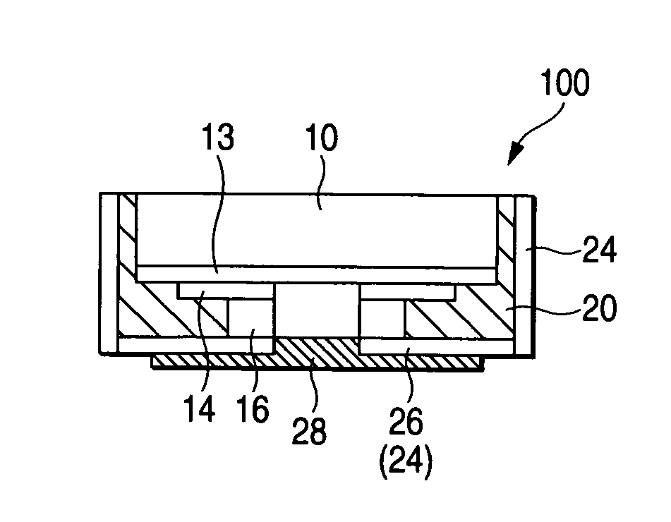
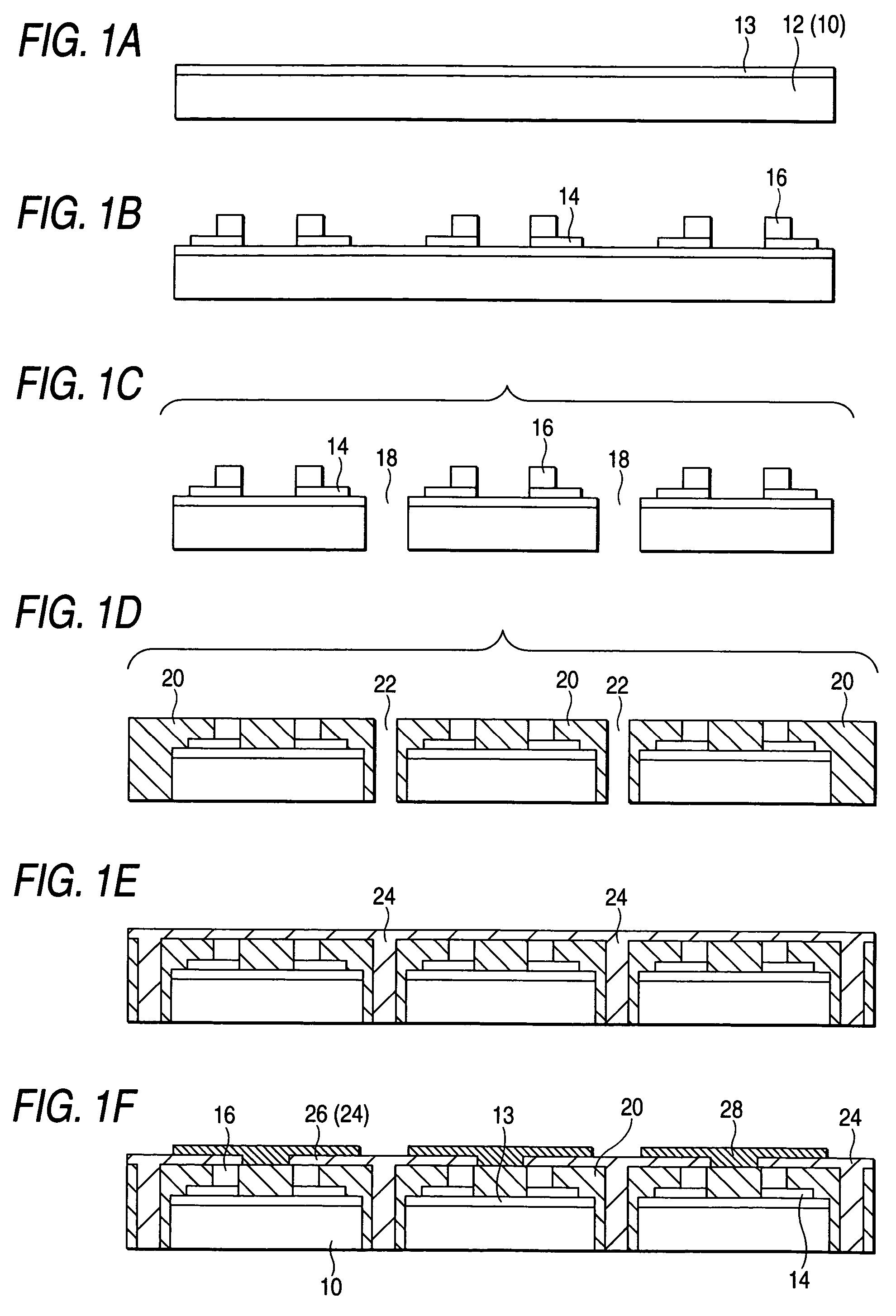
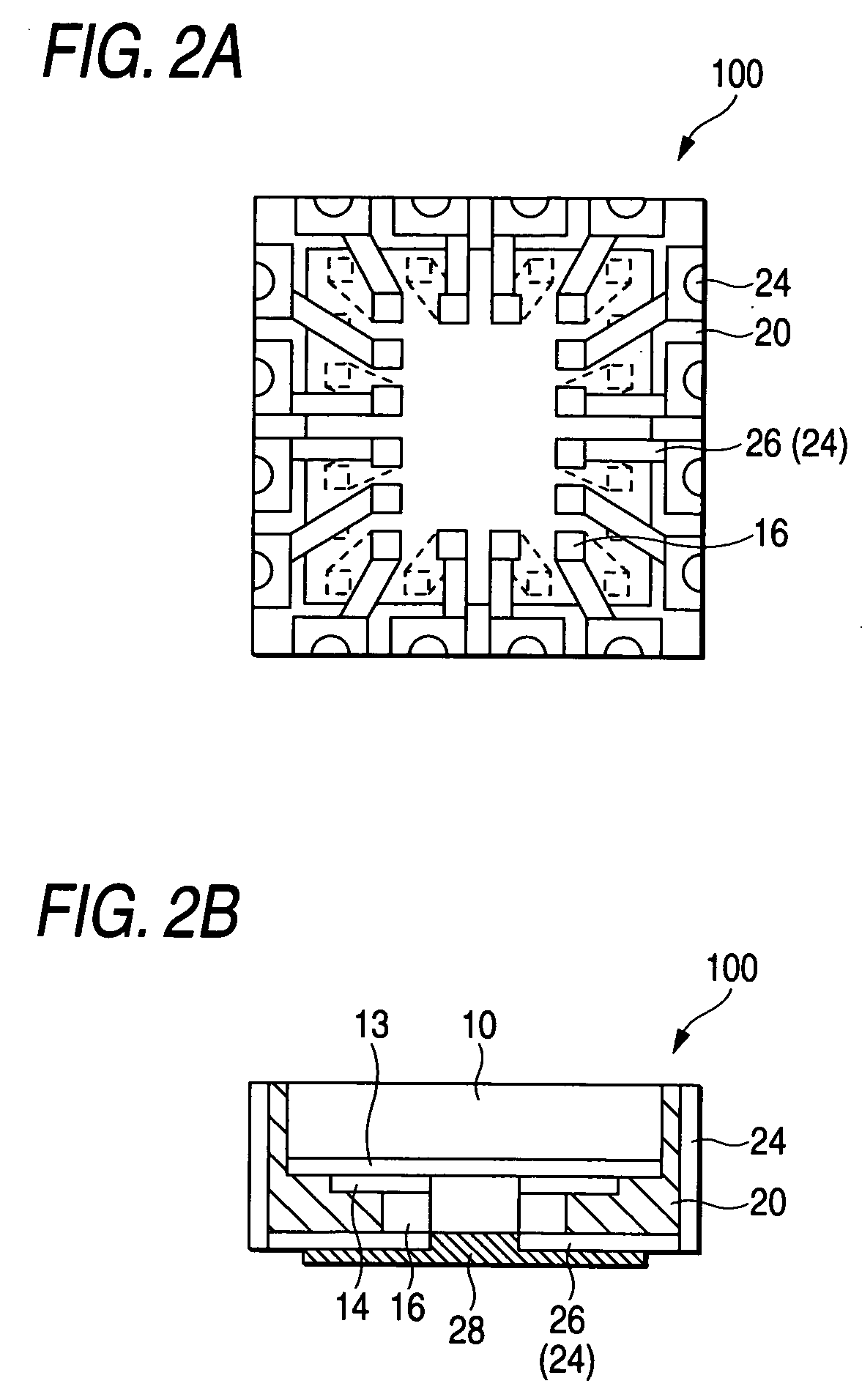
[0054]FIGS. 1A to 1F are process diagrams for illustrating a method for fabricating a semiconductor device in a first embodiment. FIGS. 2A and 2B are schematic block diagrams depicting the semiconductor device in the first embodiment; 2A is a plan view and 2B is a partial cross section.

[0055]A semiconductor device 100 in the first embodiment is configured in which an insulating material 20 is formed on the side of a semiconductor chip 10 and a conductive layer 24 (conductive pattern) and an interconnect 26 (conductive pattern) are formed to extend from the top of the front side of the insulating material 20 to posts 16 of the semiconductor chip 10. Furthermore, the semiconductor chip 10 is configured to include an insulating film 13 for protecting integrated circuits formed on the front side thereof, electrodes (electrode pads, not shown) electrically connected to the integrated circuits, a redistribution wiring layer 14 as abase for forming wiring routed from the electrodes and the...

second embodiment

[0068]FIG. 4 is a partial cross section depicting a semiconductor device in a second embodiment.

[0069]The second embodiment is the form that the semiconductor devices 100 in the first embodiment are stacked. In the embodiment, one ends of the conductive layers 24 formed on the sides of the semiconductor chips 10 are joined to each other through connecting members 30 such as solder to stack two semiconductor devices 100.

[0070]In the embodiment, since one end of the conductive layer 24 is used as a terminal, the pitch between the terminals can be set wider than that of traditional ones as described above. Therefore, connection failure is hard to occur, and highly reliable three-dimensional packaging (stack mounting) is feasible. For example, the embodiment can be utilized effectively to increase processing capacity in semiconductor devices such as memories.

third embodiment

[0071]FIG. 5 is a partial cross section depicting a semiconductor device in a third embodiment.

[0072]The third embodiment is the form that the semiconductor devices 100 in the first embodiment are stacked. In the embodiment, bar-shaped connecting materials 32 are attached to the conductive layers 24 formed on the sides of the semiconductor chips 10 with the connecting member 30 such as solder, and three semiconductor devices 100 are stacked through the bar-shaped connecting materials 32. In addition, a solder ball 36 is formed at the tip end of the bar-shaped connecting material 32 as a connecting terminal. The stacked semiconductor devices are mounted on a wiring board through the solder balls 36.

[0073]In the embodiment, connection failure is hard to occur, and highly reliable three-dimensional packaging (stack mounting) is feasible as similar to the second embodiment.

[0074]Furthermore, in the embodiment, many semiconductor devices 100 can stably undergo three-dimensional packaging...


PUM


Abstract

A semiconductor device includes a semiconductor chip having an electrode pad electrically connected to an integrated circuit and a conducting part electrically connected to the electrode pad; an insulating material formed on a side of the semiconductor chip; and a conductive pattern to extend from a top of a front side of the insulating material to the conducting part of the semiconductor chip.

Description

BACKGROUND OF THE INVENTION[0001]1. Field of the Invention[0002]The present invention relates to a small-sized semiconductor device typified by CSP (Chip Size Package) and to a method for fabricating the same.[0003]This application is counterpart of Japanese patent application, Serial Number 138584 / 2003, filed May 16, 2003, the subject matter of which is incorporated herein by reference.[0004]2. Description of the Related Art[0005]Traditionally, in integrated circuit packages having semiconductor devices such as semiconductor integrated circuits packaged, a demand for the realization of reduction in size and in thickness is increasing. In recent years, with a focus on the semiconductor integrated circuit package in the field for which the reduction in thickness is demanded particularly, CSP is proposed in which ball-shaped terminals are arranged on the surface of a semiconductor device in a grid shape.[0006]For example, the CSP is fabricated as shown in FIGS. 11A to 11D. Fist, a waf...

Claims


Application Information

Patent Timeline
Patent Type & Authority Patents(United States)
IPC IPC(8): H01L21/44H01L23/12H01L21/56H01L23/31H01L25/10H01L25/11H01L25/18
CPCH01L21/56H01L23/3114H01L24/97H01L25/105H01L21/561H01L2225/1064H01L2924/01004H01L2924/01078H01L2924/14H01L2924/30105H01L2924/01005H01L2924/01006H01L2924/01033H01L2225/1035H01L2225/1058H01L24/24H01L24/82H01L24/96H01L2224/04105H01L2224/12105H01L2224/16145H01L2224/32145H01L2224/73267H01L2224/94H01L2924/12042H01L2924/18162H01L2924/00H01L2224/03
Inventor YAMAGUCHI, TADASHI
Owner LAPIS SEMICON CO LTD
Why Eureka
Try Eureka