Electronic component, method of manufacturing the electronic component, and electronic apparatus
a manufacturing method and electronic component technology, applied in the direction of electrical apparatus casings/cabinets/drawers, coupling device connections, semiconductor/solid-state device details, etc., can solve the problems of high sensitivity, high price of components, and high cost of mounting devices, so as to reduce the price of electronic devices and simplify the mounting process , the effect of easy mounting
- Summary
- Abstract
- Description
- Claims
- Application Information
AI Technical Summary
Benefits of technology
Problems solved by technology
Method used
Image
Examples
first embodiment
[0047
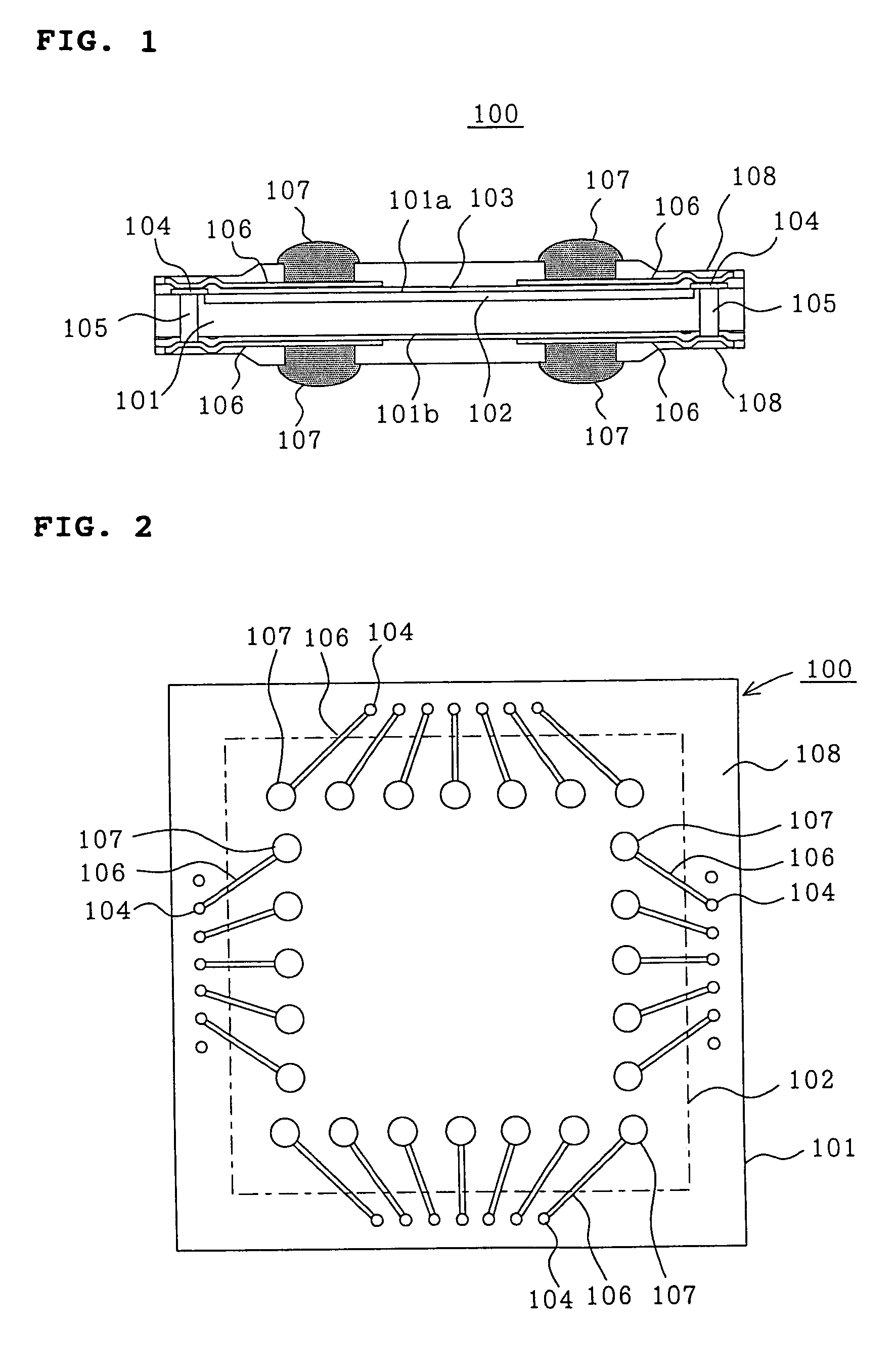
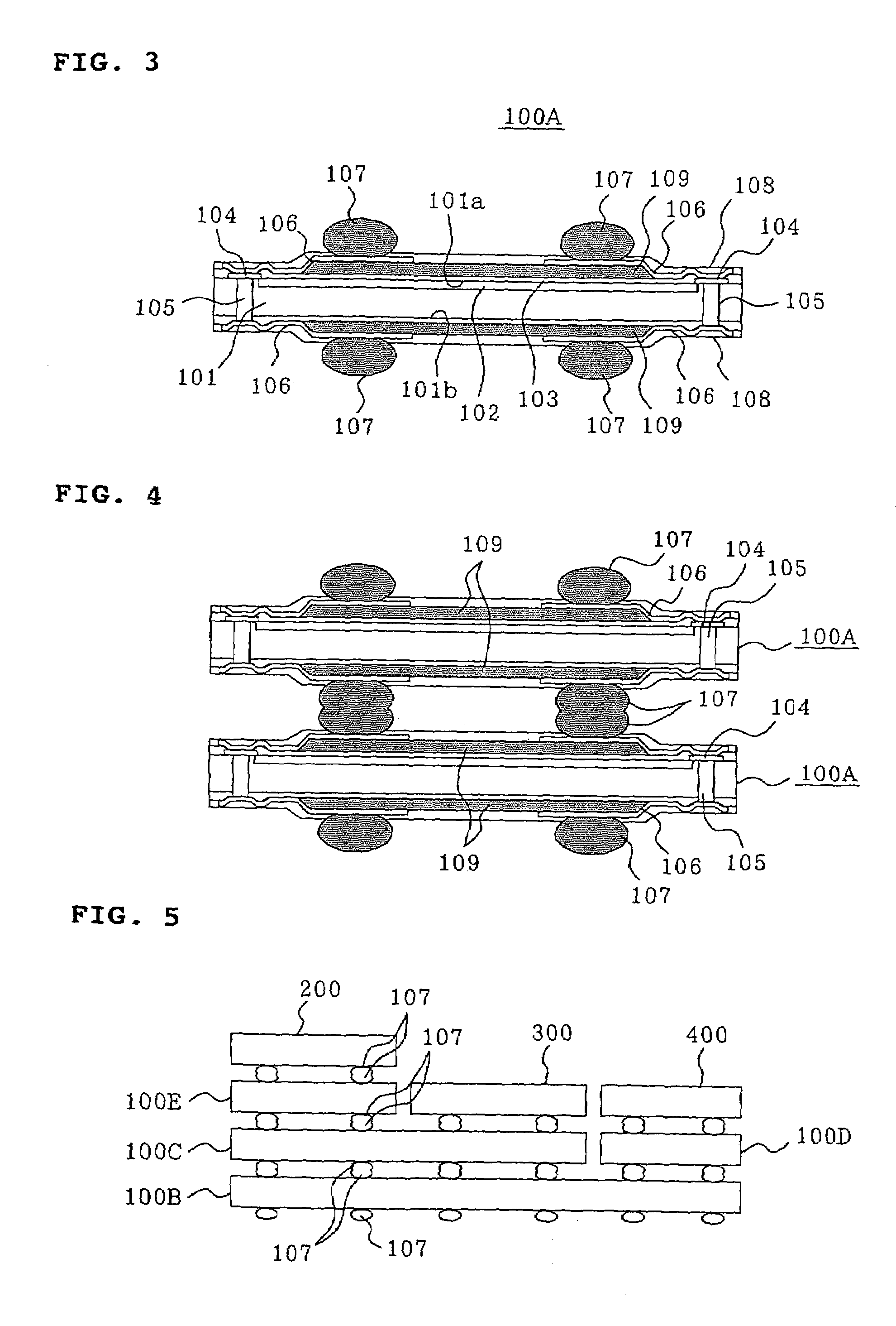
[0048]FIG. 1 is a sectional view showing the structure of a semiconductor device 100, which is an electronic component according to a first embodiment of the present invention. FIG. 2 is a plan view showing the front face of the electronic component shown in FIG. 1. The semiconductor device 100 has a silicon substrate 101. A functional part 102 is formed beneath a front face 101a of the silicon substrate 101. A passivation layer 103, made of silicon nitride (SiN), silicon oxide (SiO), or the like, is preferably formed on the functional part 102. The functional part 102 has a single active element or at least one active element and at least one passive element. In order to carry out a predetermined function, the functional part 102 performs a variety of signal processing, including arithmetic processing, image processing, speech synthesis, sound analysis, noise reduction, frequency analysis, encryption, decryption, and authentication, for input signals supplied from input termin...
second embodiment
[0058
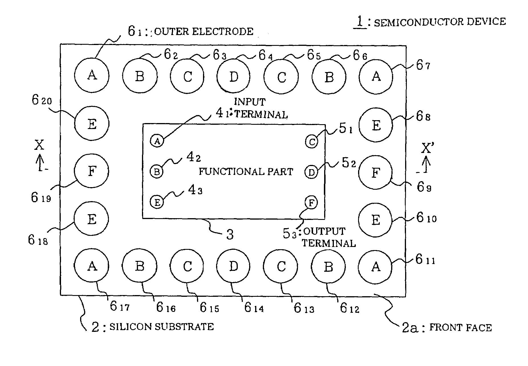
[0059]FIG. 6 is a schematic top view of a semiconductor device 1, which is an electronic component according to a second embodiment of the present invention. FIG. 7 is a schematic bottom view of the semiconductor device 1 in FIG. 6. FIG. 8 is a cross-sectional view of the semiconductor device 1 in FIG. 6 taken along line X–X′.
[0060]The semiconductor device 1 has a rectangular silicon substrate 2 and a functional part 3. The functional part 3 is formed beneath a substantially central part of a front face 2a and in the vicinity of the front face 2a of the silicon substrate 2. Outer electrodes 61 to 620 are formed near the margin of the front face 2a of the silicon substrate 2. Outer electrodes 71 to 720 are formed near the margin of a bottom face 2b of the silicon substrate 2. The outer electrodes 61 to 620 are hereinafter collectively referred to as outer electrodes 6. The same applies to the outer electrodes 71 to 720 and other components whose reference numerals have subscript...
third embodiment
[0081
[0082]FIG. 11 is a schematic cross-sectional view showing the structure of a semiconductor device 21, which is an electronic component according to a third embodiment of the present invention. The same reference numerals are used in FIG. 11 to identify the same components shown in FIGS. 6 to 8. A detailed description of such components is omitted here. In the semiconductor device 21 shown in FIG. 11, a stress relief layer 221 having a substantially trapezoidal cross section is formed on the substantially central part of the front face 2a of the silicon substrate 2. In addition, a stress relief layer 222 having the same shape as the stress relief layer 221 is formed on the substantially central part of the bottom face 2b of the silicon substrate 2. The stress relief layer 221 is plane symmetric with the stress relief layer 222 with respect a virtual plane including the midpoint between the front face 2a and the bottom face 2b of the silicon substrate 2. The stress relief layer 2...
PUM
 Abstract
Description
Claims
Application Information


