Duty ratio corrector, and memory device having the same

a duty ratio and corrector technology, applied in pulse manipulation, pulse technique, instruments, etc., can solve problems such as errors, deficient in low level, and operating margin, and achieve the effect of improving the operation speed of the second inverter

Active Publication Date: 2006-04-04
SK HYNIX INC
View PDF9 Cites 15 Cited by
  • Summary
  • Abstract
  • Description
  • Claims
  • Application Information

AI Technical Summary

Benefits of technology

[0022]The present invention is directed to a duty ratio corrector which can reduce power consumption by blocking current paths between output terminals and a ground terminal by applying input signals for turning off switching devices for generating an auxiliary voltage for correcting a duty ratio at an initial stage, and which can improve an operational speed by changing the auxiliary voltage from a predetermined voltage, not 0V, to an target voltage, and a memory device having the same.
[0031]Preferably, a capacitor is further installed between an output terminal of the first NAND gate and a ground terminal, for equalizing delay of the first input signal and the second input signal.
[0032]Preferably, a transistor being coupled between an output terminal of the second inverter and the ground terminal and having its gate coupled to an input terminal of the second inverter is further installed to improve an operational speed of the second inverter.

Problems solved by technology

In this case, an operational margin is sufficient in a high level but deficient in a low level, to generate errors.
Therefore, the current starts to flow in a standby mode or before a normal operation mode, which results in high power consumption.
However, it takes a long time to increase the auxiliary voltage DCC or DCCB to the target level, and thus takes a long time to correct the duty ratio.
As a result, it influences a lock time of a delay locked loop using the same.

Method used


Image

  • Duty ratio corrector, and memory device having the same
  • Duty ratio corrector, and memory device having the same
  • Duty ratio corrector, and memory device having the same

Examples


first embodiment

[0051]FIG. 4 is a circuit diagram illustrating a memory device having a duty ratio corrector in accordance with the present invention.

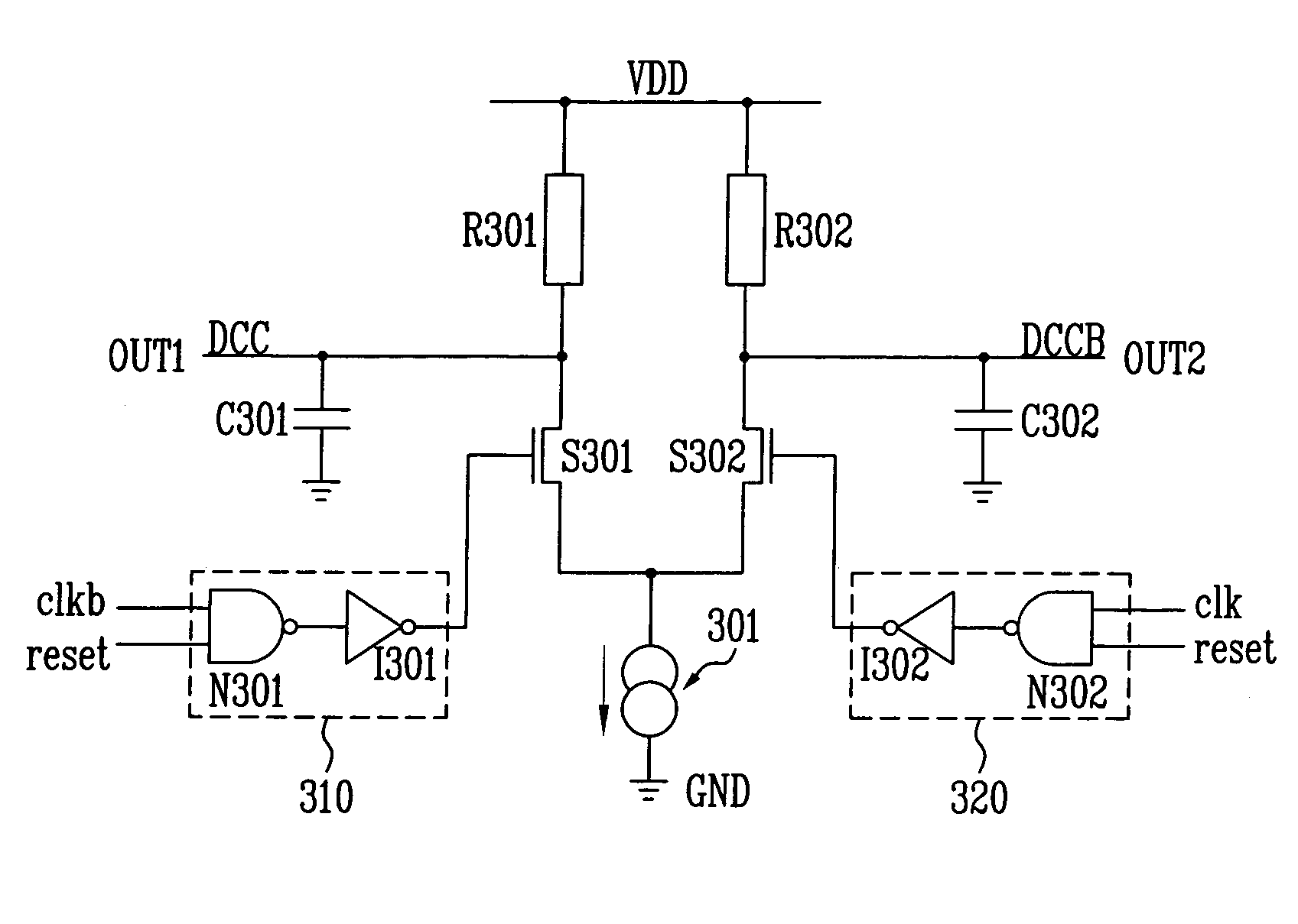
[0052]Referring to FIG. 4, when an input signal is one signal such as a clock signal, the memory device includes a phase separator 410 and a duty ratio corrector 420.

[0053]The phase separator 410 is divided into a first output unit 411 and a second output unit 412.

[0054]The first output unit 411 includes a NAND gate N401 for receiving a reset signal reset for deciding an operation or non-operation of the duty ratio corrector 420 and a clock signal clkin, and an inverter I401 for outputting a clock signal clk by inverting the output signal from the NAND gate N401. Here, a capacitor C401 can be additionally installed between an output terminal of the NAND gate N401 and a ground terminal, for equalizing delay of the clock signal clk and an inverted clock signal clkb generated in the second output unit 412. Accordingly, the first output unit 401 outputs t...

second embodiment

[0057]FIG. 5 is a circuit diagram illustrating a memory device having a duty ratio corrector in accordance with the present invention.

[0058]As illustrated in FIG. 5, when input signals are two signals inp and inn having different phases, the memory device includes a buffer 510 and a duty ratio corrector 520.

[0059]The buffer 510 includes a first NAND gate N501 for receiving a reset signal reset for deciding an operation or non-operation of the duty ratio corrector 520 and the first input signal inp, a first inverter I501 for outputting a clock signal clk by inverting the output signal from the first NAND gate N501, a second NAND gate N502 for receiving the reset signal reset and the second input signal inn, and a second inverter I502 for outputting an inverted clock signal clkb by inverting the output signal from the second NAND gate N502.

[0060]Accordingly, the buffer 510 outputs the clock signal clk and the inverted clock signal clkb according to the reset signal reset only when the...


PUM


Abstract

The present invention discloses a duty ratio corrector which can reduce power consumption by blocking current paths between output terminals and a ground terminal by applying input signals for turning off switching devices for generating an auxiliary voltage for correcting a duty ratio at an initial stage, and which can improve an operational speed by changing the auxiliary voltage from a predetermined voltage, not 0V, to an target voltage, and a memory device having the same.

Description

[0001]This application relies for priority upon Korean Patent Application No. 2004-0027096 filed on Apr. 20, 2004, the contents of which are herein incorporated by reference in their entirety.BACKGROUND[0002]1. Field of the Invention[0003]The present invention relates to a duty ratio corrector and a memory device having the same, and more particularly to, a duty ratio corrector which can minimize power consumption and rapidly generate an output signal by blocking current paths in an initial mode, and a memory device having the same.[0004]2. Discussion of Related Art[0005]All memory devices use clock signals. As an operational speed of the memory device increases, a duty ratio of an input clock signal influences performance of the whole chip. Therefore, a duty ratio corrector for maintaining a duty ratio of a clock signal at 50% has been employed.[0006]The operation of the duty ratio corrector will now be described.[0007]FIG. 1 is a concept diagram for explaining the operation of the...

Claims


Application Information

Patent Timeline
Patent Type & Authority Patents(United States)
IPC IPC(8): H03K3/017G11C8/00H03K5/151H03K5/156
CPCH03K5/1565H03K5/151A47J27/004A47J27/086A47J36/00A47J43/075
Inventor CHOI, YOUNG BAENA, KWANG JIN
Owner SK HYNIX INC
Why Eureka
Try Eureka