
Thin-film common mode filter and thin-film common mode filter array

a filter array and common-mode technology, applied in the direction of inductances, inductances with magnetic cores, coils, etc., to achieve the effect of reducing and improving the reliability of the conduction between the layers

Active Publication Date: 2006-04-04
TDK CORPARATION
View PDF7 Cites 18 Cited by
  • Summary
  • Abstract
  • Description
  • Claims
  • Application Information

AI Technical Summary

Benefits of technology

The present invention provides a thin-film common mode filter with improved reliability in the electrical connection between the drawing terminals and external-connect electrode terminals. This is achieved by a thin-film common mode filter comprising a plurality of thin-film common mode filters, each containing a pair of magnetic plates, an upper coil conductor and lower coil conductor, and an upper lead conductor and lower lead conductor. The drawing terminals are connected to the conductor layers in a way that ensures reliable electrical connection between them. The invention also provides a method for improving the reliability of the electrical connection between the drawing terminals and external-connect electrode terminals by stacking conductor layers and using through holes in the layers. The width of the lead conductor is important for high-frequency transmission properties, and the use of narrowing the width of the lead conductor improves reliability without reducing the resonance frequency. The lower and upper lead conductors are made of copper, and the surfaces of the conductors are covered with nickel / chromium films to prevent an increase in electrical resistance.

Problems solved by technology

Therefore, it has been a problem of reliability where, in some cases, the external-connect electrode terminal formed on the chip side has an incomplete electrical connection with the drawing terminal.

Method used


Image

  • Thin-film common mode filter and thin-film common mode filter array
  • Thin-film common mode filter and thin-film common mode filter array
  • Thin-film common mode filter and thin-film common mode filter array

Examples


Embodiment Construction

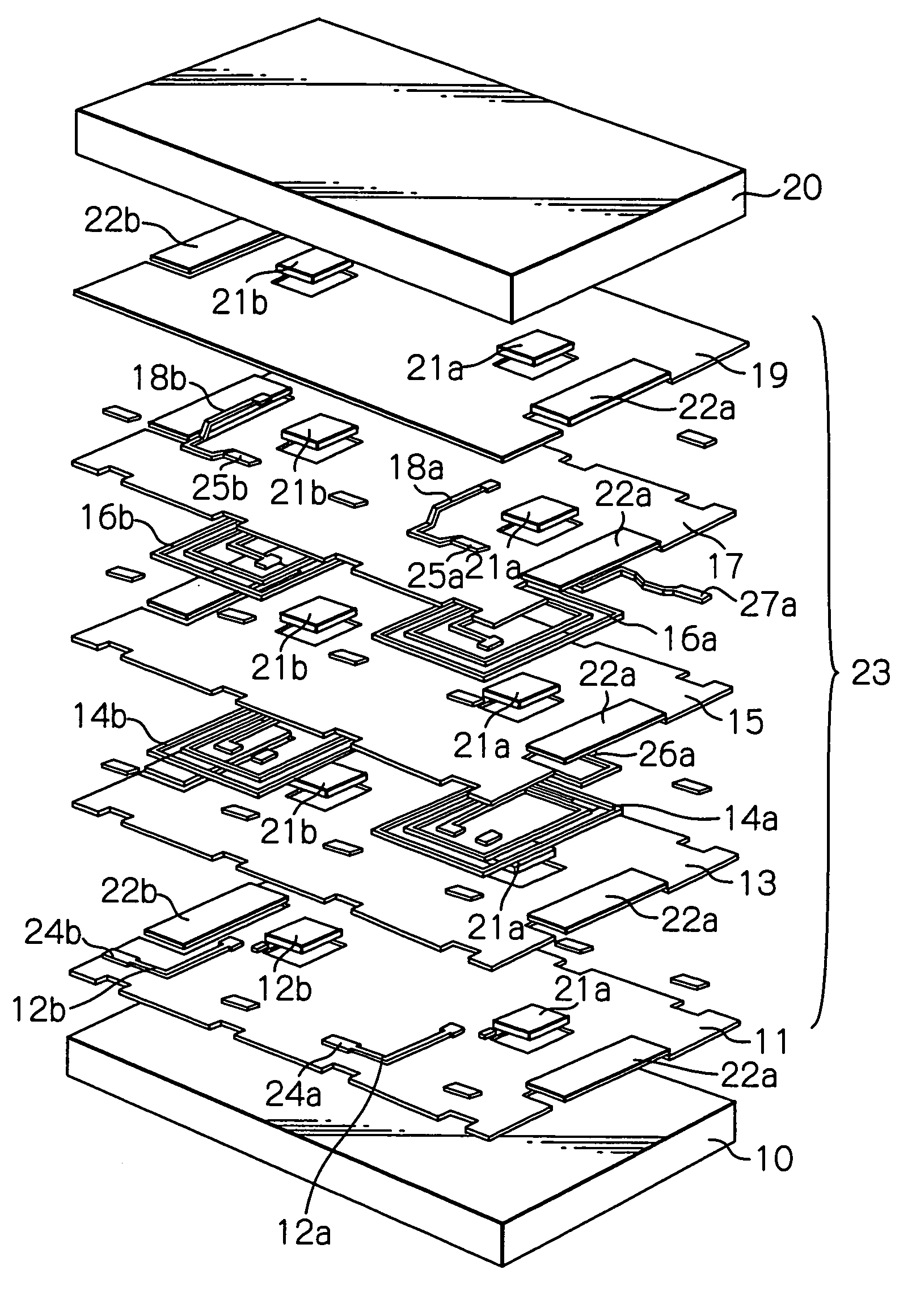
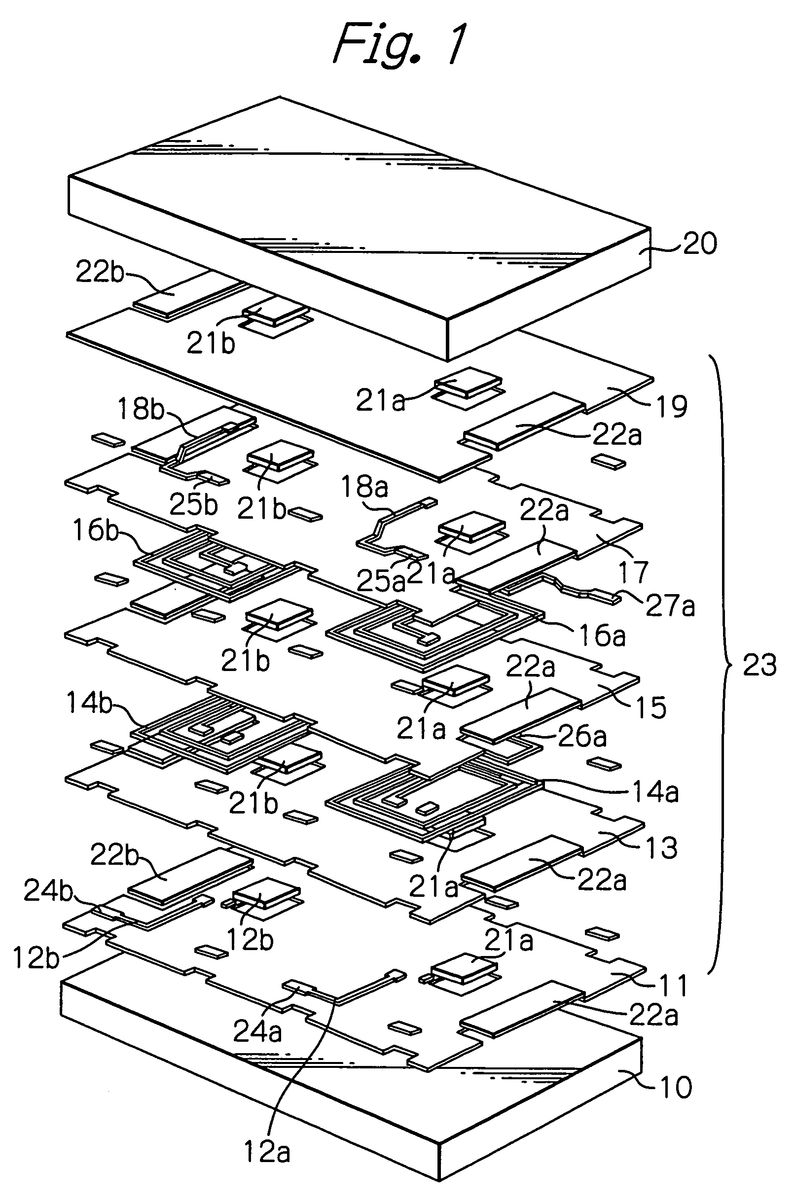
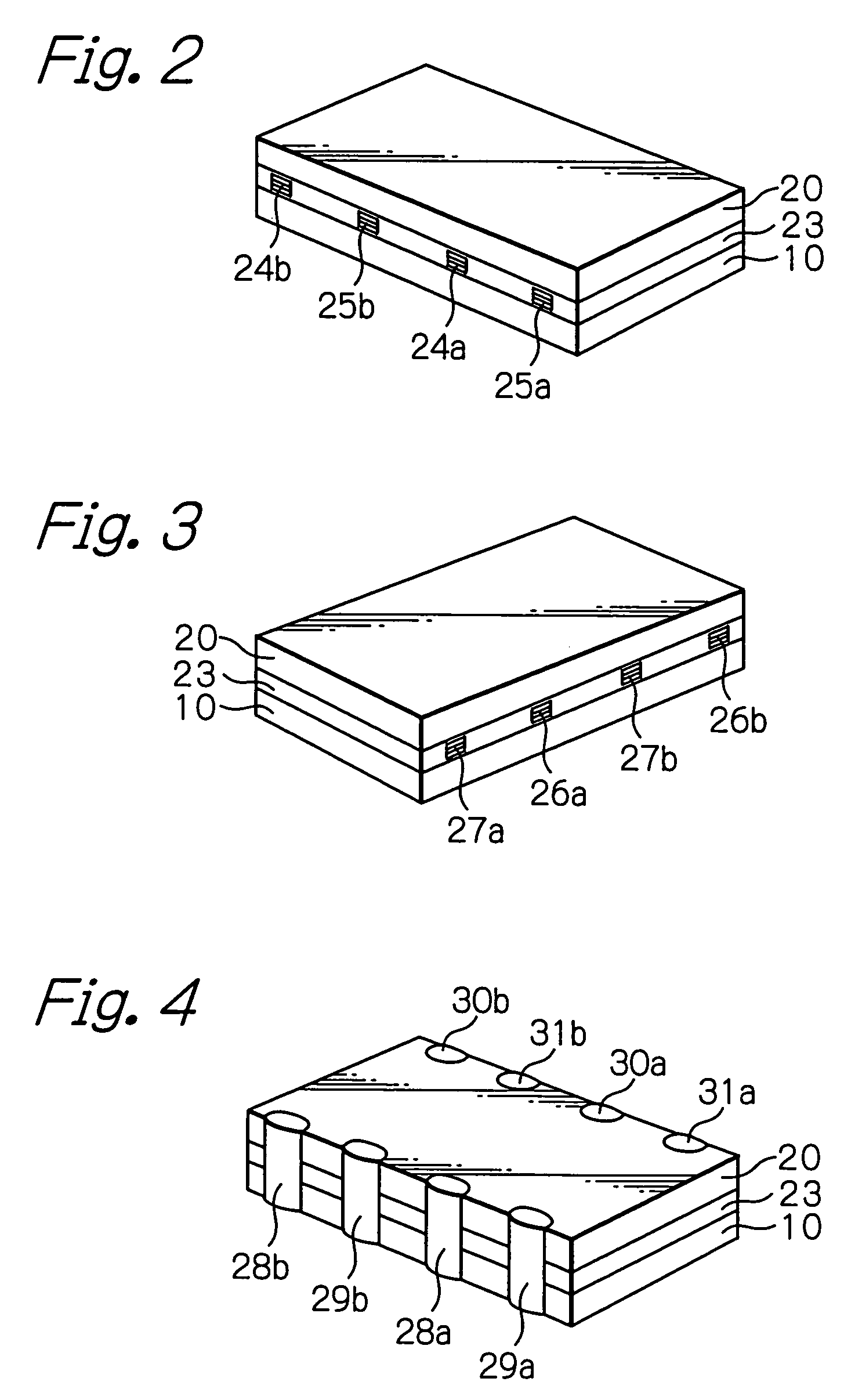
[0033]FIG. 1 shows an exploded perspective view schematically illustrating a structure of a thin-film common mode filter array according to an embodiment of the present invention. FIG. 2 shows a perspective view schematically illustrating an appearance of a thin-film common mode filter array when cut out of a wafer. FIG. 3 shows another perspective view from the different direction from that in FIG. 2, schematically illustrating an appearance of a thin-film common mode filter array when cut out of a wafer. FIG. 4 shows a perspective view schematically illustrating an appearance of a finished-up thin-film common mode filter array.

[0034]The thin-film common mode filter array is formed as a chip by aligning two thin-film common mode filters.

[0035]In FIG. 1, reference numeral 10 indicates an insulating magnetic substrate, 11 indicates a first insulating layer usually formed of a polyimide or a BCB (benzocyclobutene) that have great heat-resistance, stacked on the insulating magnetic sub...


PUM

PropertyMeasurementUnit
resonance frequencyaaaaaaaaaa
conductionaaaaaaaaaa
dimensionsaaaaaaaaaa

Abstract

A thin-film common mode filter is provided, comprising: a pair of magnetic plates; upper / lower coil conductors formed between the magnetic plates, spirally wound in the magnetic plate surface direction, overlapped each other; upper / lower lead conductors one ends of which are connected electrically to one ends in centers of the upper / lower coil conductors, respectively, extended to external portions across these coil conductors; an upper / lower lead drawing terminals to which the other ends of the upper / lower lead conductors are connected, respectively; an upper / lower coil drawing terminals to which the other ends of the upper / lower coil conductors are connected, respectively; and each of the lower lead / coil drawing terminals and the upper coil / lead drawing terminals having a structure where at least two of conductor layers to be patterned into the upper / lower lead conductors and the upper / lower coil conductors are stacked, and brought into conduction with each other.

Description

PRIORITY CLAIM[0001]This application claims priority from Japanese patent application No. 2003-398964, filed on Nov. 28, 2003, which is incorporated herein by reference.BACKGROUND OF THE INVENTION[0002]1. Field of the Invention[0003]The present invention relates to a thin-film common mode filter and a thin-film common mode filter array.[0004]2. Description of the Related Art[0005]Common mode filter is a device for suppressing common mode currents that cause electromagnetic interference in parallel transmission lines. The common mode filter has magnetically coupled inductors to remove in-phase noise component.[0006]Thin-film common mode filter miniaturized and highly integrated by forming bilayered thin-film coils between ferrite substrates and by constructing in chip form, and thin film common mode filter array on which a plurality of the filters are mounted, are described in for example, Japanese Patent Publications Nos. 04-364709A, 08-203737A, 08-335517A and 11-054326A.[0007]Gener...

Claims


Application Information

Patent Timeline
Patent Type & Authority Patents(United States)
IPC IPC(8): H03H7/01H01F5/00H01F17/00H01F17/04H01F27/29H01F37/00H03H1/00
CPCH03H7/427H01F17/0013H03H2001/0085H01F2017/0093
Inventor SHOJI, SHIGERU
Owner TDK CORPARATION
Learn More