
Exposure apparatus, exposure method and process for producing device

Inactive Publication Date: 2006-04-04
NIKON CORP
View PDF16 Cites 2 Cited by
  • Summary
  • Abstract
  • Description
  • Claims
  • Application Information

AI Technical Summary

Benefits of technology

[0013]An object of the present invention is to provide an exposure apparatus, an exposure method, and a process for production of a device in a so-called step-and-scan system exposure system enabling prevention of defocus and superior in productivity (throughput).
[0047]In the present invention, when performing scanning exposure from the outside of the substrate to the inside, by switching from control of only the focusing to control of leveling as well when the number of measurement positions or measurement points of the sensor or detecting means on the substrate increases, it is possible to prevent defocus. Further, since scanning exposure from the outside of the substrate also becomes possible, the productivity (throughput) is also improved.
[0053]That is, in the present invention in this case, the minimum length L1 required for the leveling control is set in advance. When the interval between the measurement positions of the sensor is small, the error in calculation of the plane in the leveling ends up becoming large, so it is necessary to secure a certain lateral length as the length L1. The remaining exposure length is calculated from the position intersecting the edge of the substrate enabling the lateral length L1 of the shot area to be secured and is defined as M1. The area of L1×M1 is defined as S1. On the other hand, the remaining exposure length is calculated from the position intersecting the edge of the substrate enabling the lateral length L2 of the shot area to be secured and is defined as M2. The area of L2×M2 is defined as S2. By comparing the surface areas S1 and S2 and giving priority to the larger area in selection in the sensor, it becomes possible to obtain a large area in a shot on which leveling control is performed, the accuracy of the leveling control is improved, and defocus can be further prevented. Note that when the measurement positions of the sensor are arranged at equal intervals in the non-scanning direction, it is also possible to determine the length L1 by a fixed number of measurement positions.
[0056]Note that in the present invention, it is effective to combine the invention disclosed in Japanese Patent Application No. 10-041150. That is, in a shot area before a shot area to be scanned from the outside of the substrate to the inside, the scan is performed from the inside of the substrate to the outside so as to improve the throughput. In this case, storing the position in the direction of the optical axis and tilt of the substrate at a timing when the control ends is also effective in the present invention. When starting the method of the present invention, by holding the position in the direction of the optical axis and tilt of the substrate at the timing when control at the previous shot area ended and working the method of the present invention from that state, it is possible to start the scan from a state where the focusing position and leveling plane are substantially adjusted. As a result, it is possible to shorten the time until the optimal image plane of the optical system and the actual plane of the substrate are adjusted, possible to prevent defocus, and improve the throughput as well.

Problems solved by technology

When exposing a shot area at the periphery of the wafer, however, if scanning a slit-like area irradiated by the exposure beam starting from outside the wafer, the scan is started from a location where the position in the direction of the optical axis cannot be predicted, therefore there is the problem that exposure tends to be performed in a defocused state.
Further, when exposing a shot area at the wafer periphery, the leveling control is insufficient, so there is the problem that defocus easily occurs at the time of exposure.
With this method, however, it is necessary to move for scanning in a direction opposite from the previous shot area in only shot areas at the wafer periphery and there is therefore the problem that there is inevitably a decline in the throughput.

Method used


Image

  • Exposure apparatus, exposure method and process for producing device
  • Exposure apparatus, exposure method and process for producing device
  • Exposure apparatus, exposure method and process for producing device

Examples


first embodiment

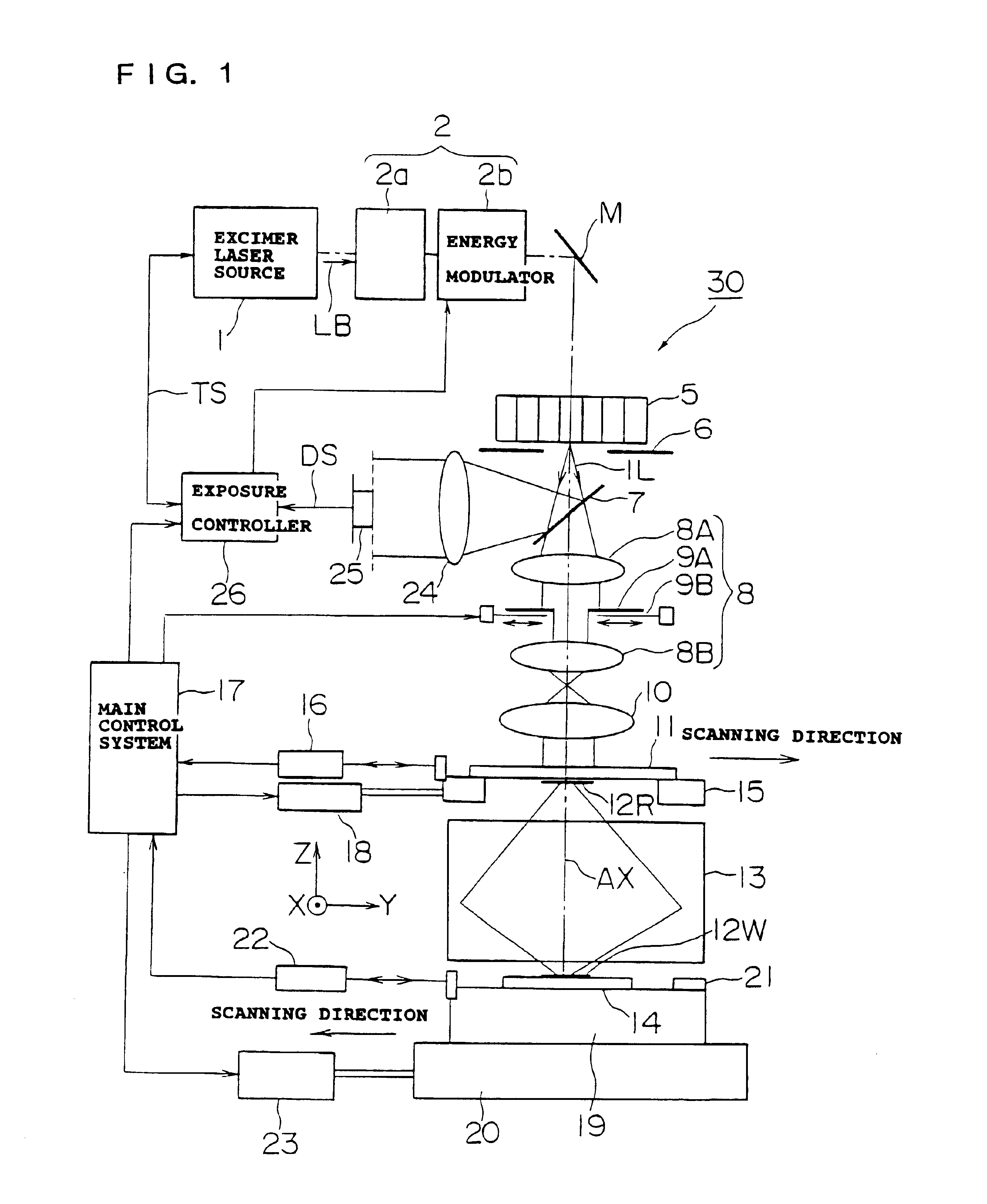
[0067]First, the overall configuration of an exposure apparatus according to a first embodiment of the present invention will be explained based on FIG. 1.

[0068]As shown in FIG. 1, the exposure apparatus 30 of the present embodiment has for example a KrF excimer laser (oscillation wavelength 248 nm) as the exposure light source 1. Note that as the exposure light source 1, it is also possible to use a metal vapor laser light source or a YAG laser harmonic generator or other pulse light source.

[0069]A light beam LB emitted in pulses from the exposure light source 1 strikes a beam shaping and modulation optical system 2. In the present embodiment, the beam shaping and modulation optical system 2 is comprised of a beam shaping optical system 2 and an energy modulator 2b. The beam shaping optical system 2a is comprised by a cylinder lens or a beam expander etc. The beam is shaped sectionally by these so as to efficiently strike the later fly-eye lens 5.

[0070]The energy modulator 2b is co...

second embodiment

[0097]The overall configuration of the exposure apparatus according to the second embodiment is similar to that of the exposure apparatus 30 shown in FIG. 1, but the technique of posture control of the Z-tilt stage 19 by the main control system 17 shown in FIG. 1 differs from the case of the embodiment shown in FIG. 4. In the following description, explanations overlapping with those of the exposure apparatus and exposure method according to the first embodiment will be partially omitted and the different portions will be explained in detail.

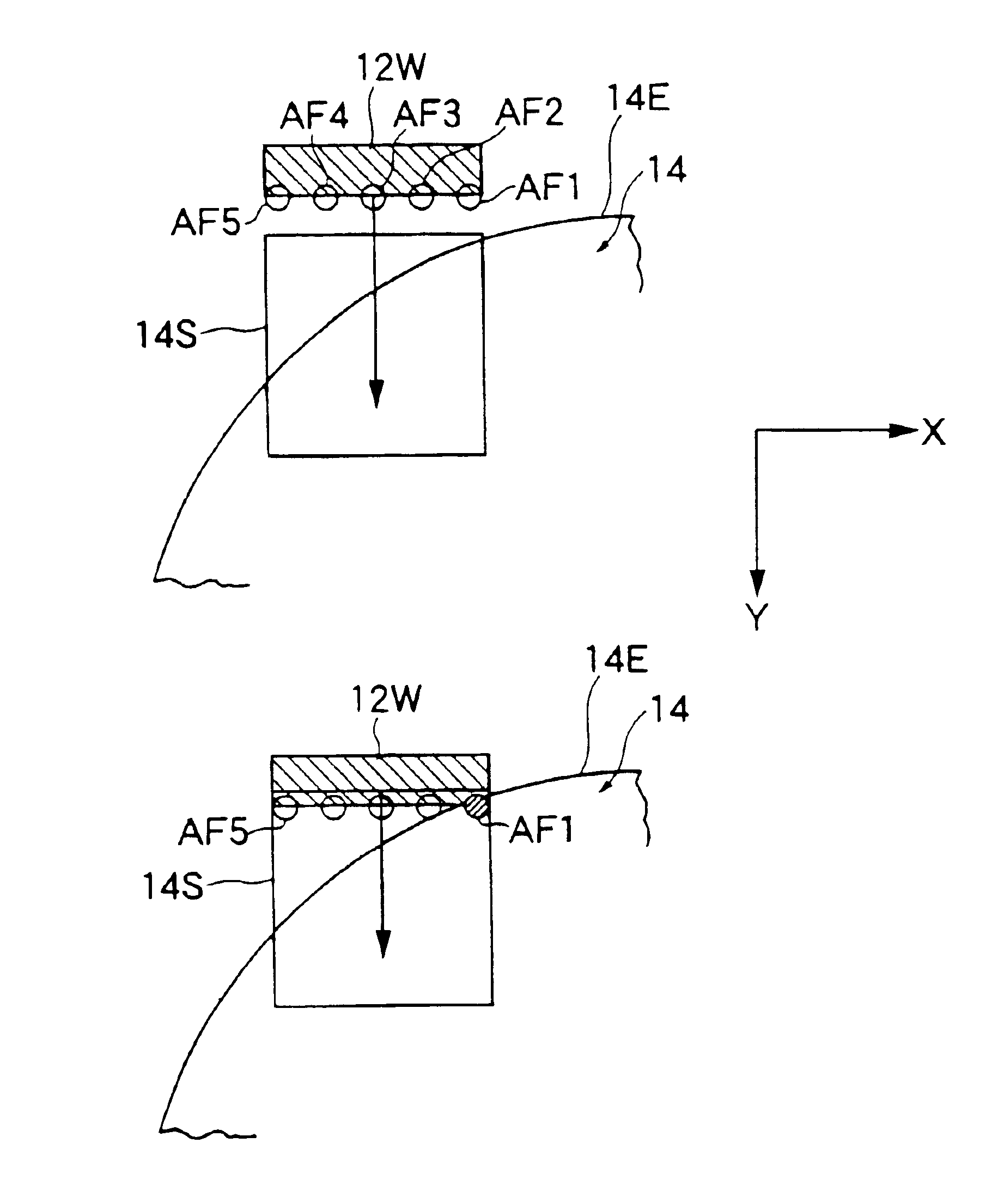
[0098]As shown in FIG. 5A, first, the system preselects measurement positions AF1 to AF5 of the row of AF sensors at the side closest to the wafer 14 first reaching the shot area 14S. Note that the five measurement positions AF1 to AF5 correspond to the five measurement positions 402-1 shown in FIG. 3A.

[0099]As shown in FIG. 5B, when the sensor AF1 reaching the surface of the wafer 14 first reaches the wafer 14, the system starts only focusing c...

third embodiment

[0102]The overall configuration of the exposure apparatus according to the third embodiment is similar to that of the exposure apparatus 30 shown in FIG. 1, but the technique of posture control of the Z-tilt stage 19 by the main control system 17 shown in FIG. 1 differs from the case of the embodiment shown in FIG. 4. In the following description, explanations overlapping with those of the exposure apparatus and exposure method according to the first embodiment will be partially omitted and the different portions will be explained in detail.

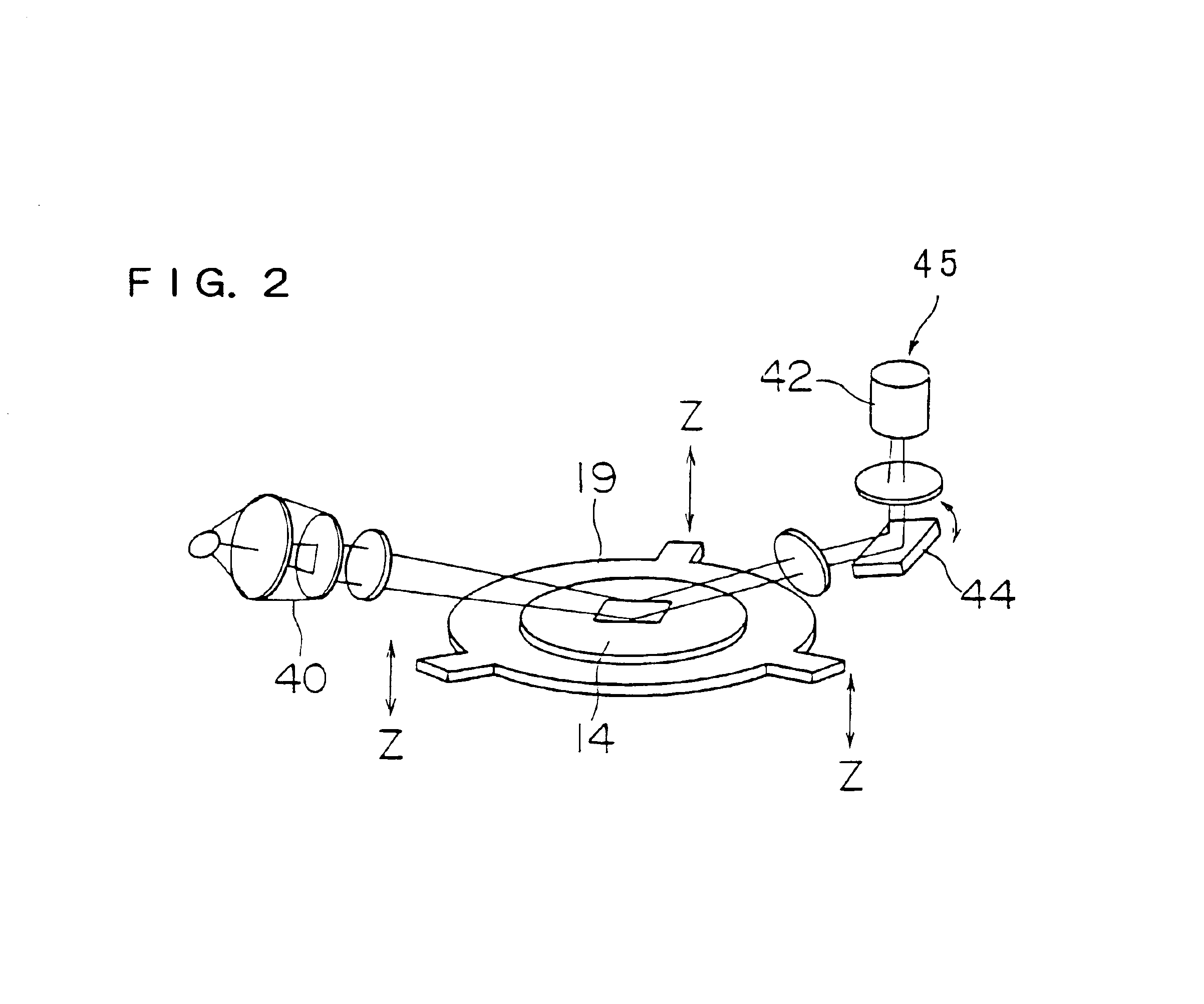
[0103]In the present embodiment, the main control system 17 shown in FIG. 1 is further provided with a determining means for determining a predetermined number df measurement positions to be selected by the AF sensor 45 shown in FIG. 2 based on which position at the periphery of the wafer 14 the shot area 14S of the wafer 14 shown in FIG. 6 is at. The predetermined measurement positions selected by the AF sensor are determined for each shot area....


PUM


Abstract

Disclosed is a step-and-scan exposure method improved in exposure at a periphery of a wafer. An area illuminated by an exposure beam is made to relatively scan a shot area positioned at the wafer periphery from the outside of the wafer to the inside. Predetermined measurement points of a sensor for detecting positional information of a wafer with respect to a focal position of a projection optical system in the direction of the optical axis of the projection optical system are made to relatively scan along with the illumination area of the exposure beam. Focus control is performed to make the wafer move in the direction of the optical axis when only part of the selected predetermined measurement positions reach the wafer, and leveling control is performed in addition to adjust the tilt of the wafer when all of the selected predetermined measurement positions reach the wafer.

Description

[0001]This is a Continuation of application Ser. No. 09 / 548,345 filed Apr. 12, 2000 now abandoned. The entire disclosure of the prior application is hereby incorporated by reference herein in its entirety.BACKGROUND OF THE INVENTION[0002]1. Field of the Invention[0003]The present invention relates to an exposure apparatus, exposure method, and process for production of a device, more particularly relates to an exposure apparatus, exposure method, and process for production of a device in so-called step-and-scan exposure able to prevent defocus at the time of exposure at a periphery of a substrate and, further, superior in productivity.[0004]2. Description of the Related Art[0005]In the lithographic process which is one of the steps in the production of a semiconductor device, as the exposure apparatus for transferring a pattern formed on a mask (including a reticle) onto a wafer coated with a photoresist, frequent use is being made of a step-and-repeat exposure apparatus for reducin...

Claims


Application Information

Patent Timeline
IPC IPC(8): G03B27/42G03B27/52G03B27/54G03F7/20G03F9/00
CPCG03F7/70358G03F9/7034G03F9/7026
Inventor WAKAMOTO, SHINJI
Owner NIKON CORP
Learn More