This helps you quickly interpret patents by identifying the three key elements:
Problems solved by technology
Method used
Benefits of technology
Benefits of technology
[0006] In order to realize distribution and product management of a large number of products by a noncontact type individual identification system using RFID tags it is necessary to attach an RFID tag to each product, and this makes mass manufacturing of RFID tags cheaply indispensable.
[0009] If the above described sandwich antenna construction is used, which encloses by an antenna each of the external electrodes formed individually on each of the faces of IC elements formed having two external electrodes each disposed individually on the respective faces that are a facing pair, the positioning between an excitation slit and each of the external electrodes formed individually on each of the faces of the IC elements must be extremely precise, and in the case of manufacturing methods of the conventional art that employs the TAB method, in order to reduce the available operating time, a method is used in which a plurality of the chips undergo suction and transportation using a plurality of vacuum suction devices. This creates problems however as complex manufacture equipment is required increasing equipment investment costs, and it is difficult to perform mass manufacture of the inlets and to achieve low costs.
[0010] In light of the above, the object of the present invention is to provide a manufacturing method for manufacturing an electronic device at low cost and with superior productivity where the device has satisfactory communication properties.
[0028] The manufacturing method for an electronic device furnishes the following effects. As IC elements having an external electrode formed respectively on each of the faces of an opposing pair are accommodated individually in a plurality of notches capable of accommodating the insertion of one of the IC elements that are arranged circumferentially around the outside of a disc shaped transport mechanism, when the disc shaped transport mechanism is rotated, a plurality of the IC elements up to a maximum number equivalent to the number of the notches, can be simultaneously delivered, thus, even when the IC elements are arranged individually on the first and second circuit layers, superior productivity can be realized and an inlet can be manufactured at a lower cost.
Problems solved by technology
In these processes, it is extremely troublesome to make the available operating time for each step occur in one second or to reduce this below one second.
This is a substantial problem affecting mass manufacture in this method and thus the TAB method has significant problems.
Further, if the available operating time is long then labor expenses increase concomitantly, mitigating against lower-cost manufacture, also as the connection between IC elements having all external electrodes formed on the same face thereof and an antenna substrate is realized using a gold-tin or gold solder connection, it is necessary to use as the substrate material, a taped substrate having copper film attached to polymide film that is expensive but strongly resistant to heat.
This makes it very difficult to manufacture the inlet economically.
This creates problems however as complex manufacture equipment is required increasing equipment investment costs, and it is difficult to perform mass manufacture of the inlets and to achieve low costs.
Method used
Image
Click on the blue label to locate the original text in one second.
Reading with bidirectional positioning of images and text.
Examples
embodiment 1
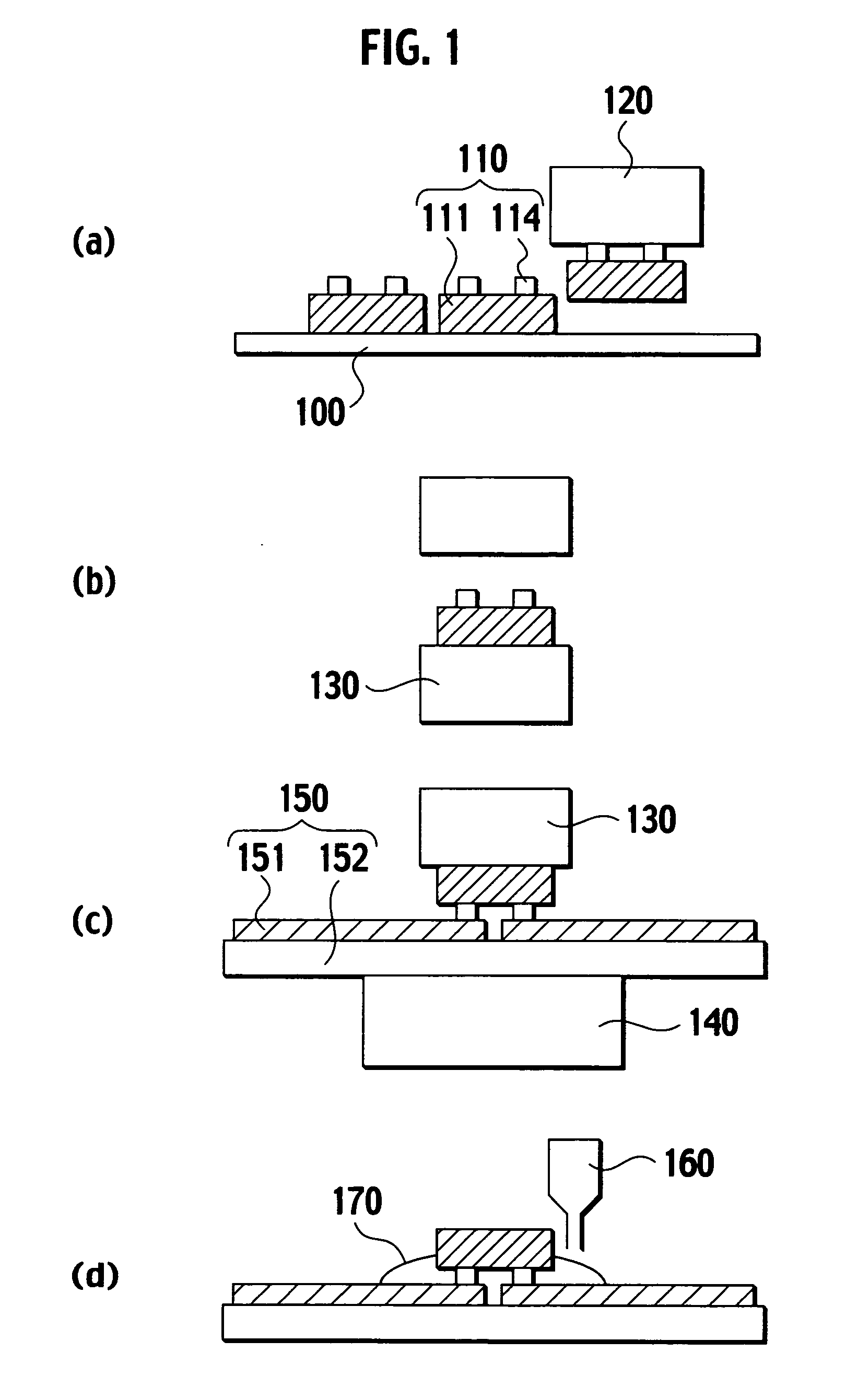
[0067] A first embodiment of the present invention will now be described with reference to FIG. 3.
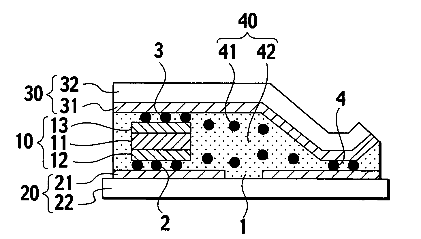
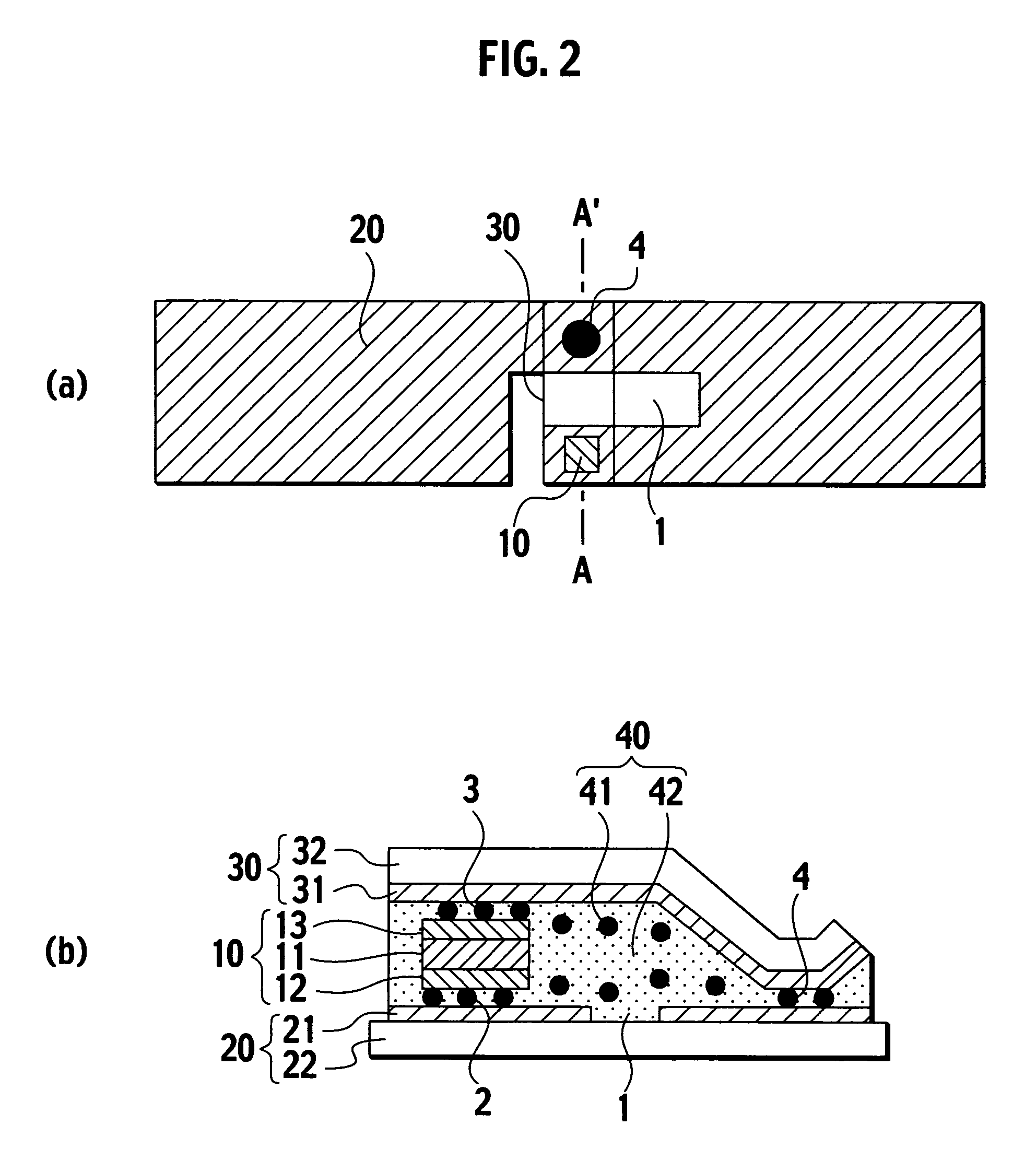
[0068] As shown in FIG. 3 (a), an etchingresist is formed by screen printing on an aluminum film surface of a tape form substrate manufactured by adhering aluminum film of a thickness of 9 μm to a polyethylene terephthalate substrate 22 of a thickness of 50 μm using an adhesive agent. Next, an antenna circuit 21 is formed continuously on the aluminum film surface using ferricchloride solution as an etching liquid. Here, the antenna thickness for each antenna circuit 21 is 2.5 mm, the thickness of the slit is 0.5 mm, and the antenna circuits 21 are formed at a pitch of 3 mm.
[0069] As shown in FIG. 3 (b), approximately 10000 IC elements 10 each having a thickness of 0.15 mm and a length and width both of 0.4 mm and having an external electrode formed respectively on the faces of each of the opposing pair of faces thereof are supplied to a high frequency parts feeder 70. The parts feed...
embodiment 2
[0078] A second embodiment of the present invention will now be described with reference to FIG. 4.
[0079] As shown in FIG. 4 (a), an etchingresist is formed by screen printing on an aluminum film surface of a tape form substrate manufactured by adhering aluminum film of a thickness of 9 μm to a polyethylene terephthalate substrate 22 of a thickness of 50 μm using an adhesive agent. Next, a continuum of antenna circuits 21 is formed on the aluminum film surface using ferricchloride solution as an etching liquid. Here, the antenna thickness for each antenna circuit is 2.5 mm, the width of the slit is 0.5 mm, and the antenna circuits are formed at a pitch of 3 mm.
[0080] Next, as shown in FIG. 4 (b) an anisotropic conductive adhesive layer is formed in the determined position on the antenna circuits 21 by lamination at a temperature of 80° C. of an anisotropic conductive adhesive film 40 (AC-2052P-45 by Hitachi Chemical) having a width of 2 mm, and then removal of the separator film...
embodiment 3
[0090] The third embodiment will now be described.
[0091] The third embodiment is the same as the second embodiment up until the steps shown in FIG. 3 (f), wherein the processing of the first circuit layer 20 is performed, an anisotropic conductive adhesive layer 40 is formed by laminating the anisotropic conductive adhesive film on the antenna circuit 21, the IC elements having external electrodes formed on the respective surfaces of the opposing pair are arranged and delivered and the IC elements are individually arranged in the determined positions on the antenna circuit 21.
[0092] Then, an anisotropic conductive adhesive film having the same width as the above anisotropic conductive adhesive film is laminated at 80° C. over those arranged IC elements, and the separator film is removed forming an anisotropic conductive adhesive layer 40.
[0093] Next, a tape form substrate 2 mm wide is prepared by adhering aluminum film of a thickness of 9 μm to a polyethylene terephthalate substr...
PUM
Abstract
A method of manufacturing an electronic device comprising IC elements 10, on a set of opposite faces of which a first electrode 12 and a second electrode 13 are formed, a first circuit layer 20 where an antenna circuit 21 having a slit 1 is formed, and a second circuit layer 30 for electrically connecting the IC elements 10 and the antenna circuit 21. The IC elements 10 are placed individually in cutouts 74, into each of which one IC element 10 can be inserted, the cutouts being formed in the outer circumference of a disk-like carrier 70. Thus, with the method, an electronic device that is inexpensive and is manufactured with high productivity, and has improved communication characteristics is manufactured.
Description
TECHNICAL FIELD [0001] The present invention relates to a manufacturing method for an electronic device like a noncontact type individual identification device providing IC elements, and more specifically a manufacturing method for manufacturing a device that furnishes excellent communication properties and that can be manufactured economically. BACKGROUND ART [0002] In recent years non-contact type individual identification systems that employee RFID (Radio Frequency Identification) tags have been focused on for use in systems for managing the entire lifecycle of a product, including all commercial aspects of manufacture of a product, its distribution and sales. Radio wave type RFID tags that use 2.45 GHz microwaves are noted for the structure that includes an external antenna attached to IC elements which enables communication to be performed over several meters. Presently, construction is ongoing of systems that operate for distribution of mass manufactured products as well as th...
Claims
Application Information
Patent Timeline
Application Date:The date an application was filed.
Publication Date:The date a patent or application was officially published.
First Publication Date:The earliest publication date of a patent with the same application number.
Issue Date:Publication date of the patent grant document.
PCT Entry Date:The Entry date of PCT National Phase.
Estimated Expiry Date:The statutory expiry date of a patent right according to the Patent Law, and it is the longest term of protection that the patent right can achieve without the termination of the patent right due to other reasons(Term extension factor has been taken into account ).
Invalid Date:Actual expiry date is based on effective date or publication date of legal transaction data of invalid patent.

