Electron beam lithography method

a lithography method and electron beam technology, applied in the direction of photomechanical equipment, maintaining head carrier alignment, instruments, etc., can solve the problems of difficult to form rectangular elements of patterns, difficult to form desired magnetization patterns in slave medium, and difficult to form good patterns, etc., to achieve high speed, shorten lithographic time, and high accuracy

Inactive Publication Date: 2006-04-11
FUJIFILM HLDG CORP +1
View PDF13 Cites 31 Cited by
  • Summary
  • Abstract
  • Description
  • Claims
  • Application Information

AI Technical Summary

Benefits of technology

[0025]In the electron beam lithography method of the present invention, the electron beam is oscillated reciprocally at high speed in the circumferential direction approximately orthogonal to the radial direction of the disk and deflected in the radial direction, thereby performing scanning of the electron beam so as to fill in the shapes of the elements. The lithography of the element

Problems solved by technology

Accordingly, it becomes difficult to form rectangular elements of a pattern.
Accordingly, it becomes difficult to form a desired magnetization pattern in a slave medium.
Therefore, good pattern formation is difficult by direct application of an electron beam lithography method using an XY stage, which is utilized in the field of semiconductors.
Moreover, in achieving a higher-capacity optical disk, since there arises a problem similar to that of the above-described master carrier for magnetic transfer, an electron beam lithography method capable of

Method used


Image

  • Electron beam lithography method
  • Electron beam lithography method
  • Electron beam lithography method

Examples


Embodiment Construction

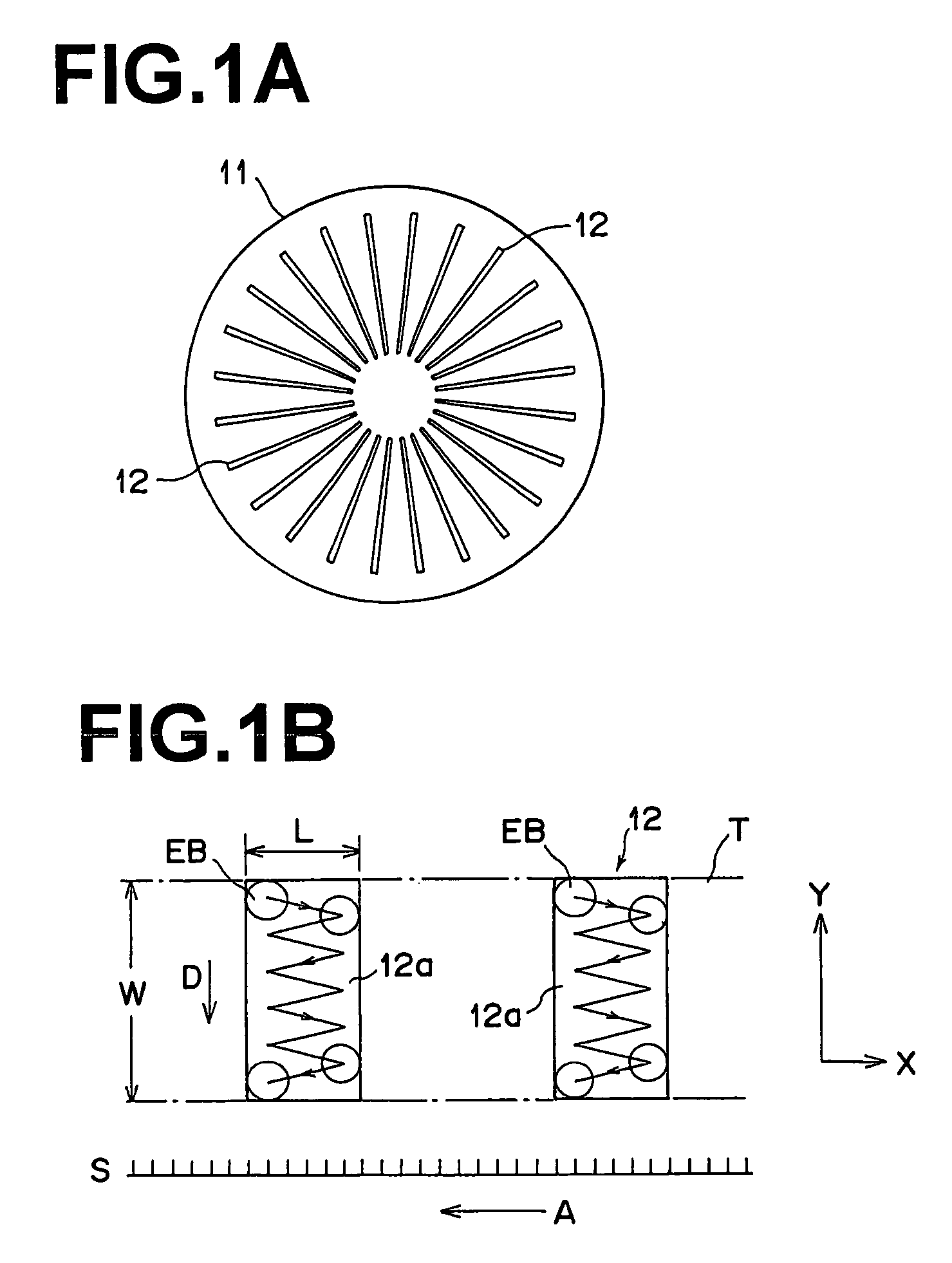
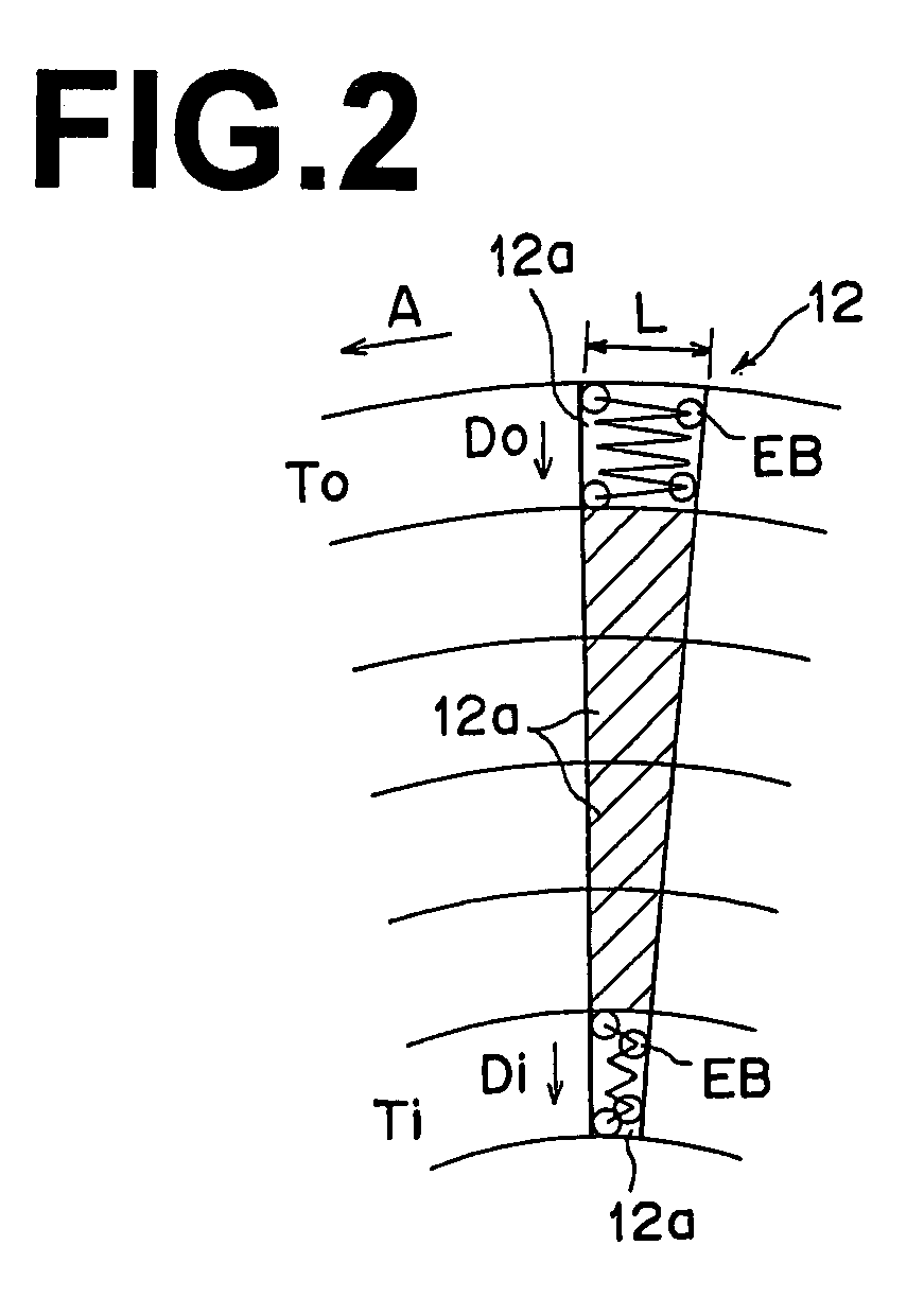
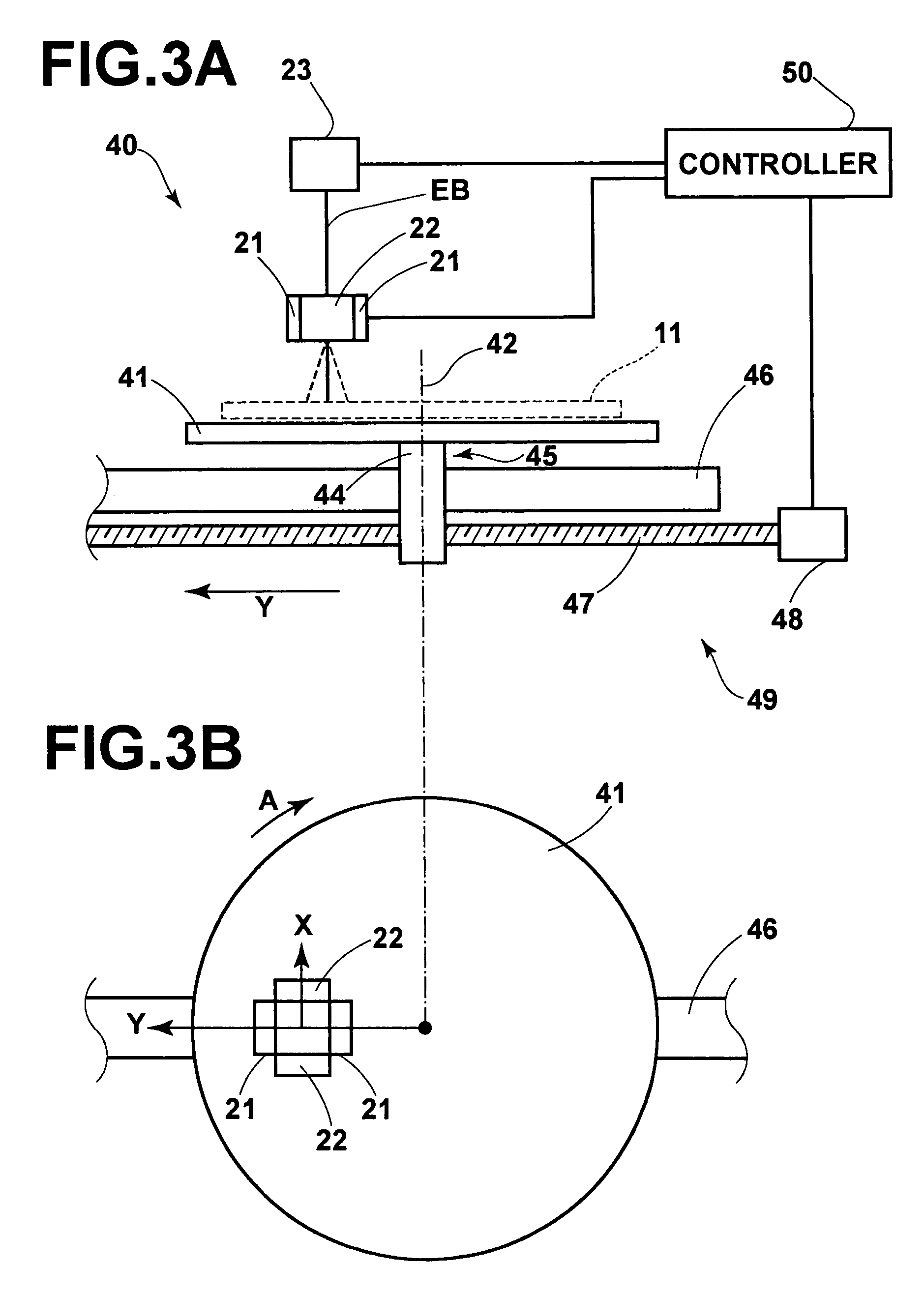
[0029]With reference to the drawings, embodiments of the present invention will be described below in detail. FIG. 1A is a plan view showing a pattern of a master carrier for magnetic transfer, which is drawn by use of an electron beam lithography method of the present invention. FIG. 1B is a magnified schematic view showing a basic lithography mode of elements included in the pattern. FIG. 2 is a magnified schematic view showing a lithography mode of the CAV type. FIGS. 3A and 3B are side and top views, respectively, of the main parts of an electron beam lithography apparatus according to an embodiment in which the electron beam lithography method of the present invention is carried out.

[0030]As shown in FIG. 1A, a pattern 12 (servo pattern) having minute irregularities formed on a master carrier for magnetic transfer is formed in a circular region excluding inner and outer periphery portions on a disk 11 (circular substrate). This pattern 12 is in the case where transfer informati...


PUM


Abstract

An electron beam lithography method for performing lithography of elements included in a pattern by scanning a disk having resist coated thereon, placed on a rotating stage which is movable in a radial direction of the disk, with an electron beam while rotating the rotating stage. The electron beam has a beam diameter smaller than a minimum width of an element shape. The electron beam is reciprocally oscillated in a circumferential direction X approximately orthogonal to a radial direction Y of the disk and deflected in the radial direction Y, thereby filling in the element shape. Lithography of the elements is sequentially performed by rotating the disk unidirectionally, and thus a desired micropattern is drawn in the entire region of the disk. A lithographic length L of the element in the circumferential direction X may be defined by amplitude of the reciprocal oscillation of the electron beam.

Description

BACKGROUND OF THE INVENTION[0001]1. Field of the Invention[0002]The present invention relates to an electron beam lithography method for performing lithography exposure of elements included in a pattern by use of an electron beam onto resist provided on a disk to form an uneven pattern and the like of a master carrier for magnetic transfer during manufacture of the master carrier for magnetic transfer and the like.[0003]2. Description of the Related Art[0004]A magnetic transfer method for transferring and recording a magnetization pattern corresponding to information (for example, servo signals) carried by a master carrier for magnetic transfer onto a slave medium is known. The magnetization pattern is transferred by applying a transfer magnetic field in a state where the master carrier and the slave medium closely contact with each other. The master carrier carries transfer information by means of a fine magnetic uneven pattern and the slave medium has a magnetic recording part for...

Claims


Application Information

Patent Timeline
IPC IPC(8): G03C5/00G11B5/82H01J37/20G03F7/20G11B5/596G11B5/84G11B5/86G11B7/26G11B7/28H01J37/147H01J37/305H01J37/317
CPCB82Y10/00B82Y40/00G03F7/2059G11B5/743G11B7/261H01J37/3174G11B5/86Y10S430/143G11B5/865G11B2020/1282G11B7/28
Inventor KOMATSU, KAZUNORIUSA, TOSHIHIRO
Owner FUJIFILM HLDG CORP
Why Eureka
Try Eureka