Systems and methods for low leakage strained-channel transistor

a technology of strained channels and transistors, applied in the field of semiconductor devices, can solve the problems of affecting the mobility of other carriers, affecting the mobility of electrons, and affecting the mobility of holes, and achieve the effect of selectively applying strain to channel regions to facilitate semiconductor device fabrication

Active Publication Date: 2006-04-11
TEXAS INSTR INC
View PDF13 Cites 82 Cited by
  • Summary
  • Abstract
  • Description
  • Claims
  • Application Information

AI Technical Summary

Benefits of technology

[0008]The present invention facilitates semiconductor device fabrication by inducing strain, relatively deeply, into channel regions of semiconductor devices. The present invention employs multiple recess structures that can have varied dopant type, dopant profile, and / or compositions in order to maintain or facilitate device operation while also selectively applying strain to channel regions.

Problems solved by technology

The drawback of this technique is that a given orientation that would be beneficial to one carrier type (e.g., holes) would not benefit the other carrier mobility.
One drawback to improving channel mobility via strain is that compressive strain, which generally improves hole mobility for silicon substrate devices, can degrade electron mobility and that tensile strain, which improves electron mobility for silicon substrate based devices, can also degrade hole mobility.
As a result, introducing tensile strain can improve performance of NMOS devices but degrade performance of PMOS devices.
Similarly, introducing compressive strain can improve performance of PMOS devices but degrade performance of NMOS devices.

Method used


Image

  • Systems and methods for low leakage strained-channel transistor
  • Systems and methods for low leakage strained-channel transistor
  • Systems and methods for low leakage strained-channel transistor

Examples


Embodiment Construction

[0017]One or more implementations of the present invention will now be described with reference to the attached drawings, wherein like reference numerals are used to refer to like elements throughout, and wherein the illustrated structures are not necessarily drawn to scale. The invention provides transistor structures and methods in which transistor mobility is improved.

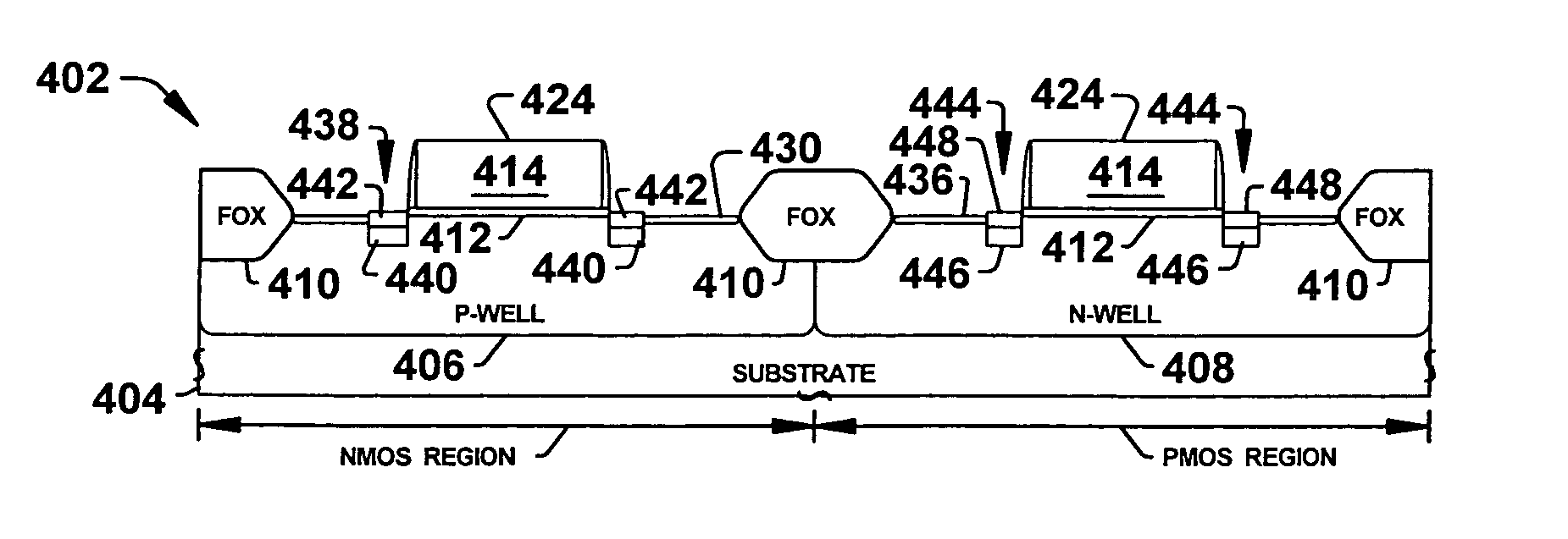
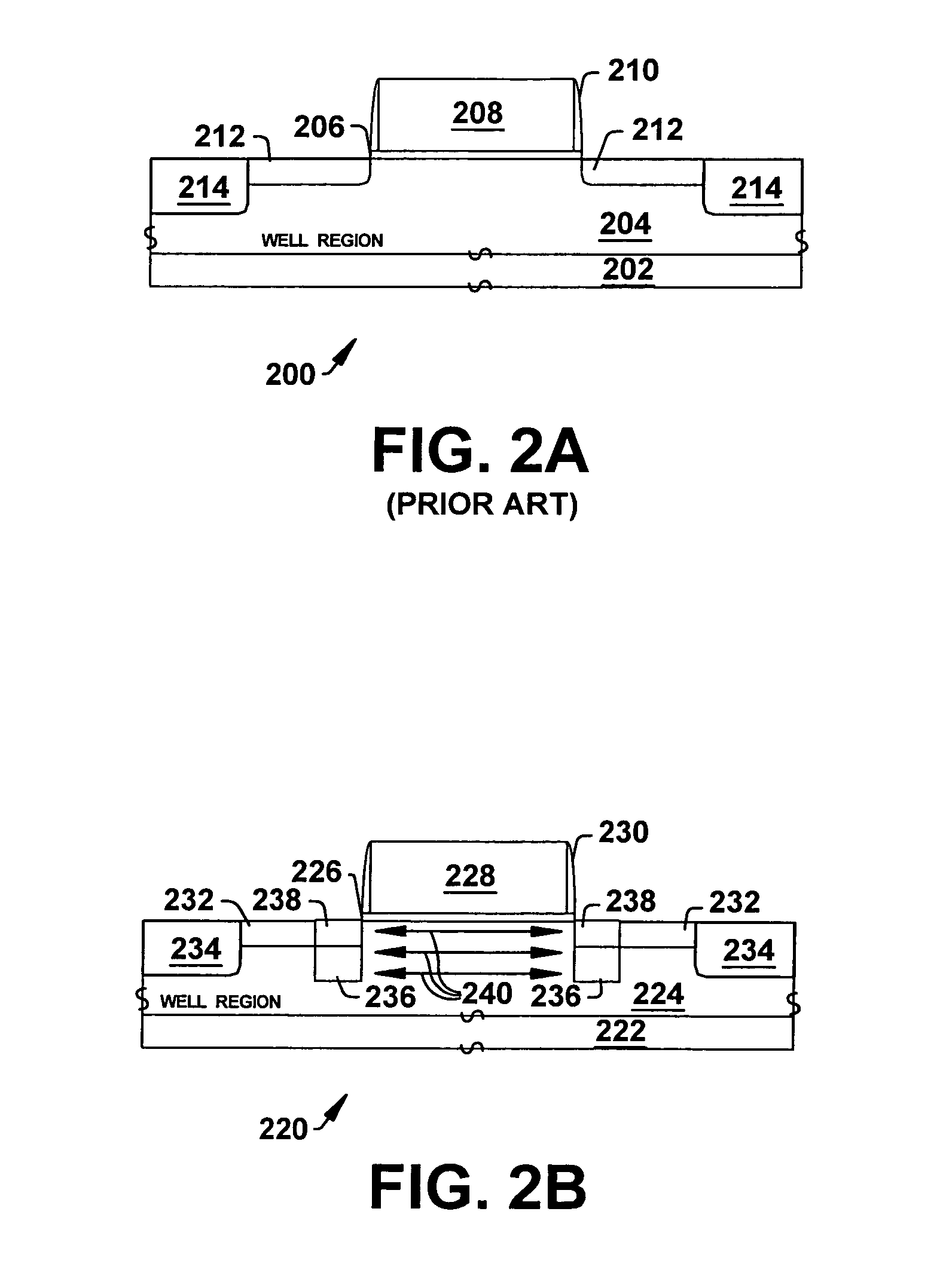
[0018]The present invention facilitates semiconductor device fabrication by inducing strain, relatively deeply, into channel regions of semiconductor devices. The present invention employs multiple recess structures that can have varied dopant type, dopant profile, and / or compositions in order to maintain or facilitate device operation while also selectively applying strain to channel regions. The multiple recess structures, by employment of strain inducing materials and dopant implanted, can apply strain to channel regions relatively deeply while mitigating leakage.

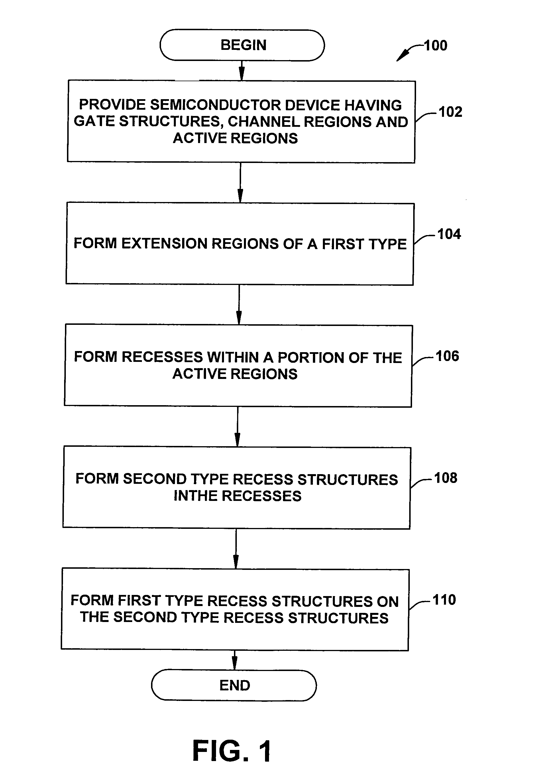
[0019]FIG. 1 is a flow diagram illustrating a meth...


PUM


Abstract

The present invention facilitates semiconductor fabrication by providing methods of fabrication that mitigate leakage and apply strain to channel regions of transistor devices. A semiconductor device having gate structures, channel regions, and active regions is provided (102). Extension regions of a first type of conductivity are formed within the active regions (104). Recesses are then formed within a portion of the active regions (106). Second type recess structures are formed (108) within the recesses, wherein the second type recess structures have a second type of conductivity opposite the first type and are comprised of a strain inducing material. Then, first type recess structures are formed (110) within the recesses and on the second type recess structures, wherein the first type recess structures have the first type of conductivity and are comprised of a strain inducing material.

Description

FIELD OF INVENTION[0001]The present invention relates generally to semiconductor devices and more particularly to transistor devices and associated methods of manufacture having improved mobility due to channel strain.BACKGROUND OF THE INVENTION[0002]A conventional MOS transistor generally includes a semiconductor substrate, such as silicon, having a source, a drain, and a channel positioned between the source and drain. A gate stack composed of a conductive material (a gate conductor), a dielectric layer (a gate oxide), and sidewall spacers, is typically located above the channel. The gate oxide is typically located directly above the channel, while the gate conductor, generally comprised of polycrystalline silicon (polysilicon) material, is located above the gate oxide. The sidewall spacers protect the sidewalls of the gate conductor and define the source and drain placement relative to the gate.[0003]Generally, for a given electric field across the channel of a MOS transistor, th...

Claims


Application Information

Patent Timeline
Patent Type & Authority Patents(United States)
IPC IPC(8): H01L21/3205H01L21/336H01L21/4763H01L21/76
CPCH01L21/823807H01L29/7848H01L29/66636H01L21/823814
Inventor KOONTZ, ELISABETH MARLEYPACHECO ROTONDARO, ANTONIO LUIS
Owner TEXAS INSTR INC
Why Eureka
Try Eureka