Method for calibrating a digital-to-analog converter and a digital-to-analog converter

a digital-to-analog converter and digital-to-analog converter technology, applied in the field of integrated electronic circuits, can solve the problems of only affecting the cumulating of systematic errors, systematic errors, and systematic errors, and achieve the effect of minimising the error in the resultant analog signal

Inactive Publication Date: 2006-04-11
VIVO MOBILE COMM CO LTD
View PDF9 Cites 16 Cited by
  • Summary
  • Abstract
  • Description
  • Claims
  • Application Information

AI Technical Summary

Benefits of technology

[0029]The invention describes a method for digitally calibrating a segmented current-steering D / A-converter. One embodiment of the present invention is a 14-bit DAC, where 6 MSB's are converted with two unweighted switchable current source array. Further, in this invention a new method for organising the switching order based on the analysed data of mismatch of the current sources is presented. A programmable mapping device is used instead of the fixed thermometer decoding before the switch array. Using this programmable mapping device the switching order of the current switches can be selected optimally so that the error in resulting analog signal is minimised. The switching order is programmed to the mapping device on the basis of the calibration method according to the present invention.
[0031]Thanks to the calibration method of the present invention the new design of the DAC does not have any effect on the analog parts of the current DAC's. Therefore there is no risk of decreasing the dynamic performance of the DAC by implementing the calibration. Further, the calibration method according to the present invention does not increase the complexity of the analog part of the DAC since everything is done in the digital part of the DAC. In fact the use of the digital calibration method makes it possible to design the DAC to be fully optimised for the high frequency performance. Also the analog area of the DAC can be kept small, which is also an advantage for the high-frequency behaviour.

Problems solved by technology

Though there are methods to design a current-steering DAC to fulfil a 14-bit DC-linearity with some yield, the high frequency behaviour becomes unacceptable.
In addition to the random mismatch there is also some systematic errors that are mainly caused by process related gradients and voltage drops in the supply lines.
However, the switching order randomising affects only the systematic error cumulating.
Also the shape of the cumulating error affects the dynamic performance.
Especially if the INL curve is heavily bowed, the DC-non-linearity can increase the distortion.
On the other hand, the large INL error increases the quantization noise.
However, if the DAC is designed to fill the DC-linearity specification, the high frequency behaviour is typically bad, because this leads to non-optimal design for high frequency signals.
The drawbacks of these prior-art solutions are as follows.
The use of parallel arrays can average these random errors, but the circuit complexity still decreases the high frequency performance.
Also, since the random mismatch is a function of the transistor area and overdrive voltage, designing a high resolution DAC consumes both area and power.
The most important issue, however, is that the designing for full DC-linearity decreases the high-frequency behaviour.
Therefore, these DAC's are typically not suitable for high-speed operation.
The dynamic element matching method spreads the DC-linearity errors into the noise floor, and therefore the errors still exists even though the distortion is low.
The use of current source that can be trimmed increases the complexity of the analog parts in the DAC, and therefore the DAC is not easy to be optimised for high frequency performance.
The prior art calibration methods are sensitive to the changes in the biasing or ambient temperature.
If the additional DAC or current sources are used in the calibration, the complexity of the analog part is further increased.
These methods also lead to problems in high-frequency operation, since the penalty is an imbalance in the main DAC.
This makes the design of the analog more complex and remarkably affects the high frequency linearity of the analog side.
On the other hand, moving the maximum deviations near the zero- and full-scale codes, the limiting of the signal swing can always decrease the effect of the DC errors from the signal.

Method used


Image

  • Method for calibrating a digital-to-analog converter and a digital-to-analog converter
  • Method for calibrating a digital-to-analog converter and a digital-to-analog converter
  • Method for calibrating a digital-to-analog converter and a digital-to-analog converter

Examples


Embodiment Construction

[0052]Reference will now be made in detail to the embodiments of the present invention, examples of which are illustrated in the accompanying drawings.

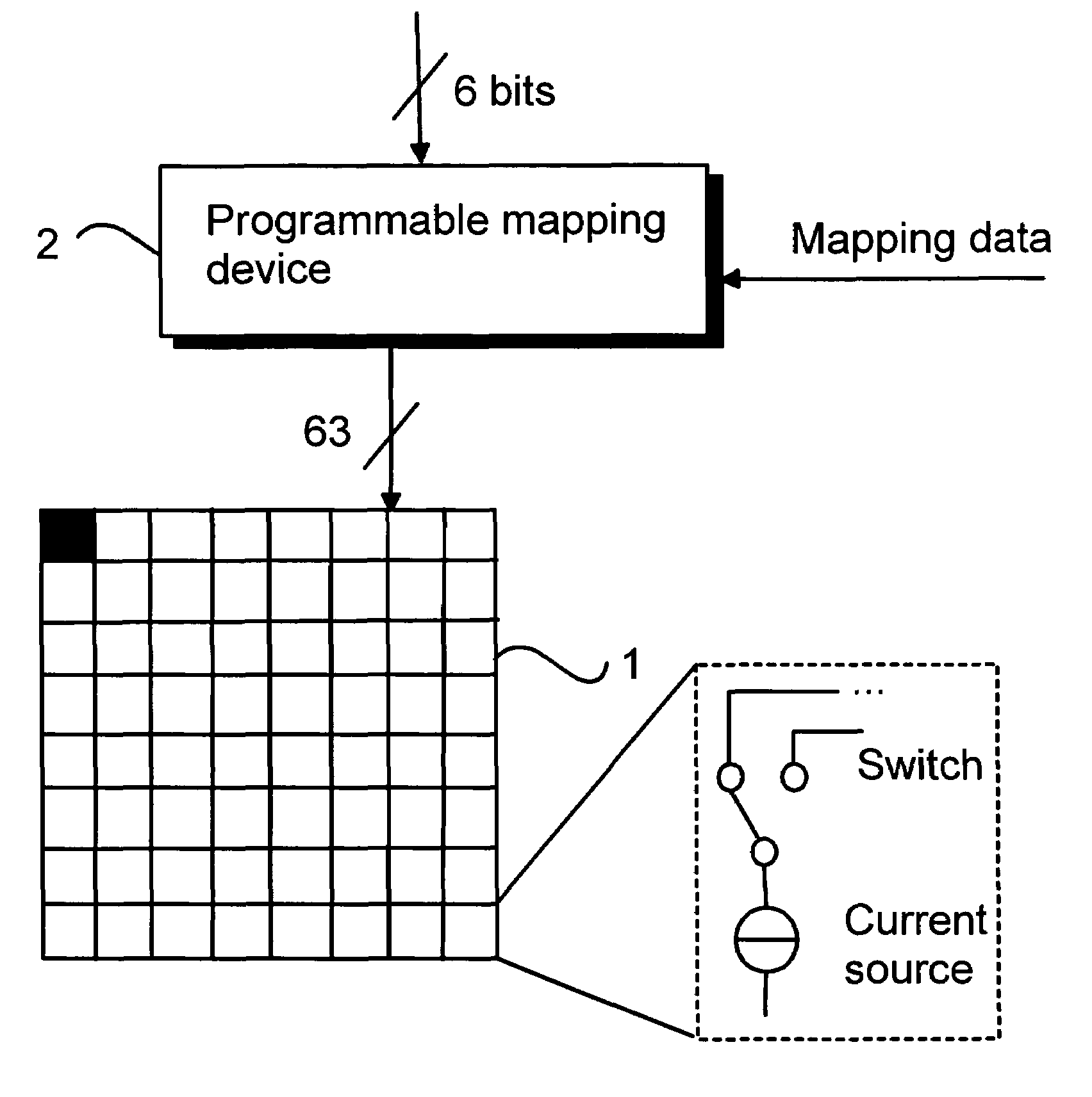
[0053]In this invention a new method for organising the switching order of the switchable current sources based on the analysed data of mismatch in said current sources is presented. In FIG. 6 is disclosed a block diagram disclosing a simplified principle example of the switchable current source array 1 that can be calibrated. Switchable current source means for example a combination of a current source and a switching element which together form a switchable current source. FIG. 6 also shows a programmable mapping device 2 which is used instead of the conventional thermometer decoder. The mapping device 2 is connected to the current switch array 1 in order to control the switching order of the current switches in the current switch array 1. In this example the mapping device can map any of the 6-bit input signals into any combination...


PUM


Abstract

The invention describes a method for digitally calibrating a segmented current-steering D / A-converter. One embodiment of the present invention is a 14-bit DAC, where 6 MSB's are converted with two unweighted current source array. Further, in this invention a new method for organising the switching order based on the analysed data of mismatch of the current sources is presented. A programmable mapping device is used instead of the fixed thermometer decoding before the switch array. Using this programmable mapping device the switching order of the current switches can be selected optimally so that the error in the resulting analog signal is minimised. The switching order is programmed to the mapping device on the basis of the calibration method according to the present invention. The inventive amendment is aimed at processing errors which cause poor matching inside the component itself. This amendment is done by rearranging unweighted unity current switches into a more optimum order.

Description

[0001]This is a Continuation of International Application No. PCT / FI02 / 00454 filed May 27, 2002, which designated the U.S. and was published under PCT Article 21(2) in English.FIELD OF THE INVENTION[0002]The present invention relates to integrated electronic circuits. In particular, the present invention relates to a novel and improved method for calibrating an unweighted current source array of a segmented current-steering D / A-converter and to a novel and improved D / A-converter design implementing said calibration method.BACKGROUND OF THE INVENTION[0003]Digital-to-analog converters are widely used for converting digital signals to corresponding analog signals for many electronic circuits. For example, a high resolution, high speed digital-to-analog converter (DAC) may find applications in cellular base stations, wireless communications, direct digital frequency synthesis, signal reconstruction, test equipment, high resolution imaging systems and arbitrary waveform generators, for e...

Claims


Application Information

Patent Timeline
Patent Type & Authority Patents(United States)
IPC IPC(8): H03M1/10H03M1/68H03M1/74
CPCH03M1/0651H03M1/1033H03M1/747H03M1/687H03M1/682H03M1/10H03M1/70
Inventor ELORANTA, PETRI
Owner VIVO MOBILE COMM CO LTD
Why Eureka
Try Eureka