Plasma processing apparatus, and electrode structure and table structure of processing apparatus

a processing apparatus and electrode technology, applied in the field of processing apparatuses, can solve the problems of deterioration of heat transfer efficiency, circuit element or structure damage, sealing gas leakage,

Inactive Publication Date: 2006-04-25
TOKYO ELECTRON LTD
View PDF37 Cites 115 Cited by
  • Summary
  • Abstract
  • Description
  • Claims
  • Application Information

AI Technical Summary

Benefits of technology

[0012]It is an object of the present invention to provide an improved and useful

Problems solved by technology

In such kinds of processes, in a case in which there is no element or arrangement or member that receives a thermal damage in a wafer such as a case in which an oxidation film is deposited on a bare wafer, there is no problem if a heat treatment is performed at a high temperature of, for example, 800° C. to 900° C. However, for example, when an interlayer insulating film or the like is formed to make a circuit element to be multilayer, there is a problem in that a circuit element or structure is damaged if a wafer is heated to a high temperature of 800° C. to 900° C. as mentioned above.
In such a high temperature range, there is a problem in that a sealed gas leaks due to deterioration of the se

Method used


Image

  • Plasma processing apparatus, and electrode structure and table structure of processing apparatus
  • Plasma processing apparatus, and electrode structure and table structure of processing apparatus
  • Plasma processing apparatus, and electrode structure and table structure of processing apparatus

Examples


Embodiment Construction

[0066]A description will be given below, with reference to the drawings, of a plasma processing apparatus according to an embodiment of the present invention.

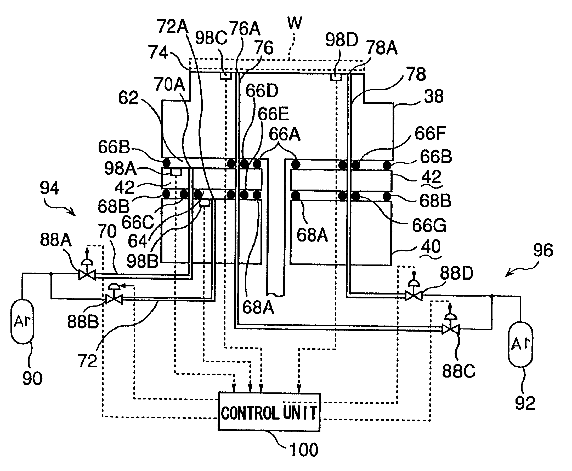
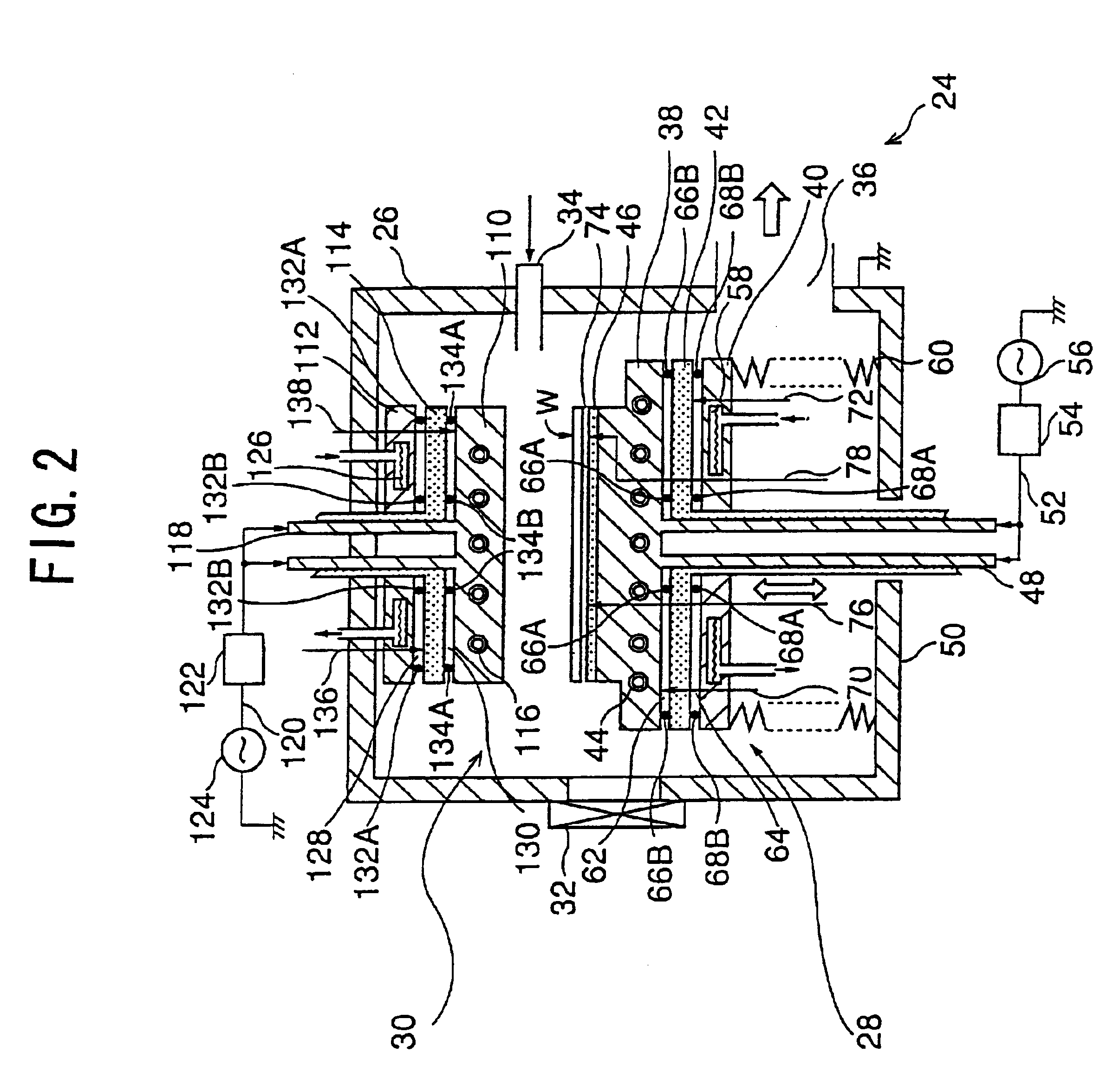
[0067]FIG. 2 is structural view of a plasma processing apparatus according to an embodiment of the present invention. FIGS. 3A though 3E are cross-sectional views of heat resistant metal seal members. FIG. 4 is a view showing a heat-transfer gas supply system of the embodiment of an electrode structure (lower electrode unit side) according to the present invention. FIG. 5 is an illustrative view of a structure of a heat resistant pressure sensor. FIG. 6 is an illustration showing a heat transfer gas supply system of the embodiment of the electrode structure (upper electrode unit side) according to the present invention.

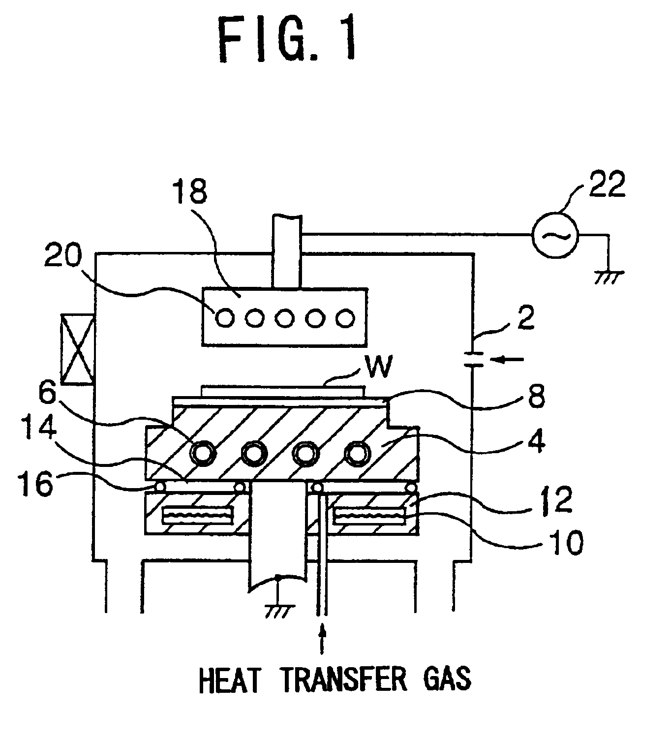
[0068]As shown in the figures, the plasma processing apparatus 24 has, for example, an aluminum made cylindrical process chamber 26. On the bottom side of the process chamber, there is provided a lower electrode ...


PUM

PropertyMeasurementUnit
Temperatureaaaaaaaaaa

Abstract

An electrode structure used in a plasma processing apparatus which performs a predetermined process on an object (W) to be processed by using a plasma in a process chamber (26) in which a vacuum can be formed. An electrode unit (38) has a heater unit (44) therein. A cooling block (40) having a cooling jacket (58) is joined to the electrode unit (38) so as to cool the electrode unit. A heat resistant metal seal member (66A, 66B) seals an electrode-side heat transfer space (62, 64) formed between the electrode unit and the cooling block. Electrode-side heat transfer gas supply means (94) supplies a heat transfer gas to the electrode-side heat transfer space. Accordingly, a sealing characteristic of the electrode-side heat transfer space does not deteriorate even in a high temperature range such as a temperature higher than 200° C. and, for example, a range from 350° C. to 500° C., and the heat transfer gas does not leak.

Description

[0001]This is a continuation of International Application Ser. No. PCT / JP00 / 04011, filed Jun. 20, 2000, which, in turn, is based on Japanese Patent Application Nos. 11-173613, filed Jun. 21, 1999, and 2000-168297, filed Jun. 5, 2000.TECHNICAL FIELD[0002]The present invention relates to a processing apparatus such as a plasma processing apparatus and, more particularly, to a structure of an electrode and a structure of a placement table that are suitable for the plasma processing apparatus.BACKGROUND ART[0003]Generally, in a manufacturing process of a semiconductor integrated circuit, various processes, such as a film deposition process, an etching process or an oxidation-diffusion process, are repeatedly performed with respect to a semiconductor wafer, which is an object to be processed. In such kinds of processes, in a case in which there is no element or arrangement or member that receives a thermal damage in a wafer such as a case in which an oxidation film is deposited on a bare...

Claims


Application Information

Patent Timeline
IPC IPC(8): C23C16/509C23F1/00H01L21/306C23C16/46H01L21/00H01L21/205H01L21/302H01L21/3065H01L21/31H01L21/683
CPCC23C16/46H01L21/67109H01J2237/2002C23C16/505
Inventor KOMINO, MITSUAKISASAKI, YASUHARUTSUBOI, KYOAMANO, HIDEAKI
Owner TOKYO ELECTRON LTD
Why Eureka
Try Eureka