Carbide emitter mask etch stop

a carbide emitter and mask technology, applied in the field of semiconductor devices, can solve the problems of poor etch selectivity, diffusion difficulties, and hinder the control of the gain and emitter area of bipolar transistors, so as to improve the control of the beta of the bipolar device, improve the matching capability of the device, and mitigate the isotropic etch effect.

Inactive Publication Date: 2006-04-25
INTEL CORP
View PDF6 Cites 6 Cited by
  • Summary
  • Abstract
  • Description
  • Claims
  • Application Information

AI Technical Summary

Benefits of technology

[0014]The present invention advantageously allows improvement in control over bipolar device beta and area as well as improved device matching capabilities through methods for forming emitter-base contact openings. A SiC layer is employed between upper and lower oxide layer as part of an emitter-base dielectric stack, and RIE etching through the upper oxide layer and the SiC layer are performed with etch selectivities beyond those possible using a conventional nitride etch stop layer. Improved etch stop capabilities, in turn, allow thinner oxide layers overlying the base layer in bipolar transistors, so as to mitigate the isotropic etch effects of the final wet etch process employed to open the emitter-base contact opening, while providing protection for the base layer from adverse effects of the anisotropic (e.g., RIE) etch processes. A better etch stop layer will also reduce the chances of over etching into the base layer. The improvement in the anisotropic nature of the removal of material to form the emitter-base contact opening allows better control of the dimensions and electrical characteristics of the emitter-base junction. This, in turn, facilitates better control over the transistor gain (e.g., beta), improved matching of bipolar transistors in a device die, and improved repeatability of the manufacturing process.

Problems solved by technology

The inventors have found that the conventional dielectric stack suffers from isotropic etch effects in wet etching the lower oxide layer in the base-emitter dielectric stack (e.g., stack 14 of FIG. 1), which hinder efforts at controlling the gain and emitter area of bipolar transistors.
In this regard, it is believed that poor etch selectivity for REI etching the upper oxide layer (e.g., layer 16) and the nitride layer (e.g., layer 20) prevent optimization of the final wet etch in forming the emitter-base contact opening, instead requiring a fairly thick lower oxide layer in the base-emitter dielectric stack to compensate for the RIE overetch needed to fully etch through the nitride layer.
In addition, it is believed that beta and area control is further exacerbated in the conventional device 30 of FIG. 1 by isotropic etch behavior in the thick lower oxide layer etch, causing diffusion difficulties in forming the emitter-base junction after implantation of the emitter structure.

Method used


Image

  • Carbide emitter mask etch stop
  • Carbide emitter mask etch stop
  • Carbide emitter mask etch stop

Examples


first preferred embodiment

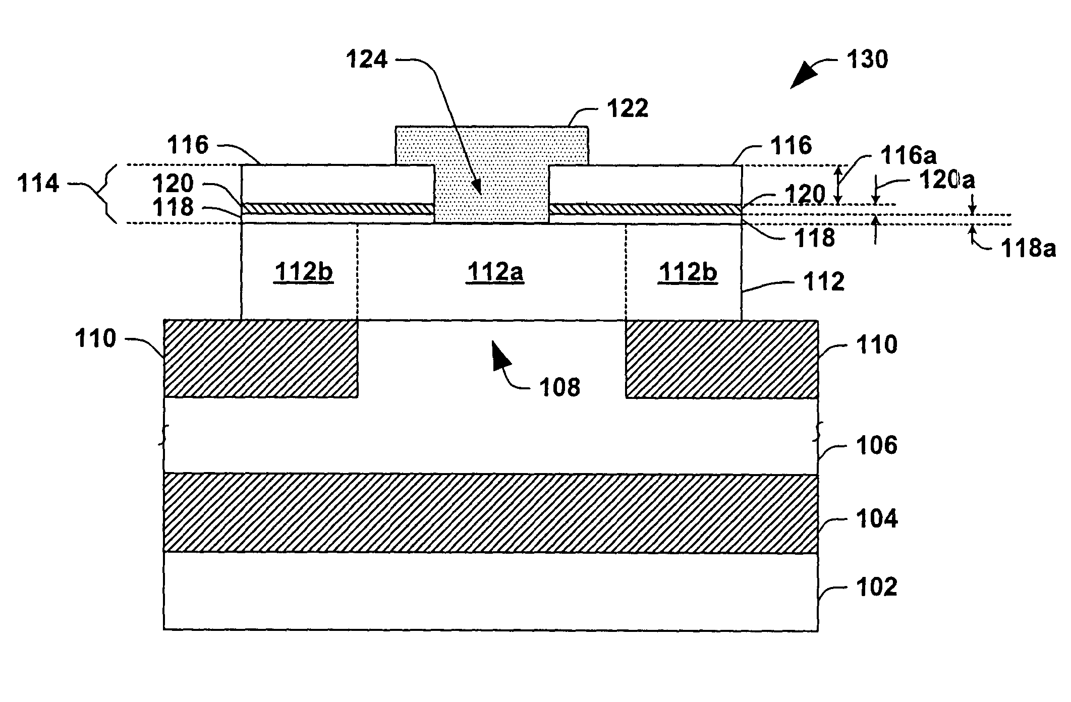
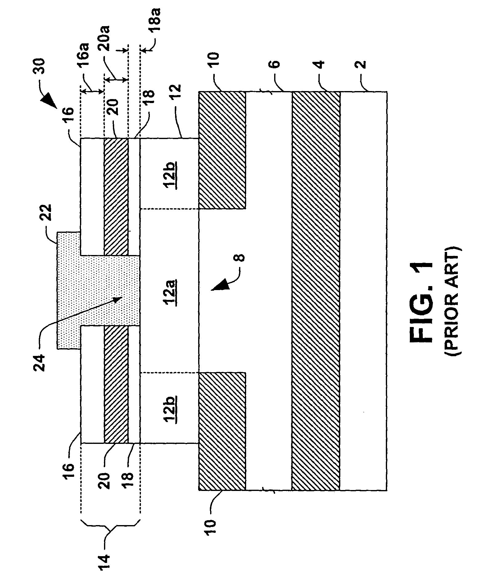
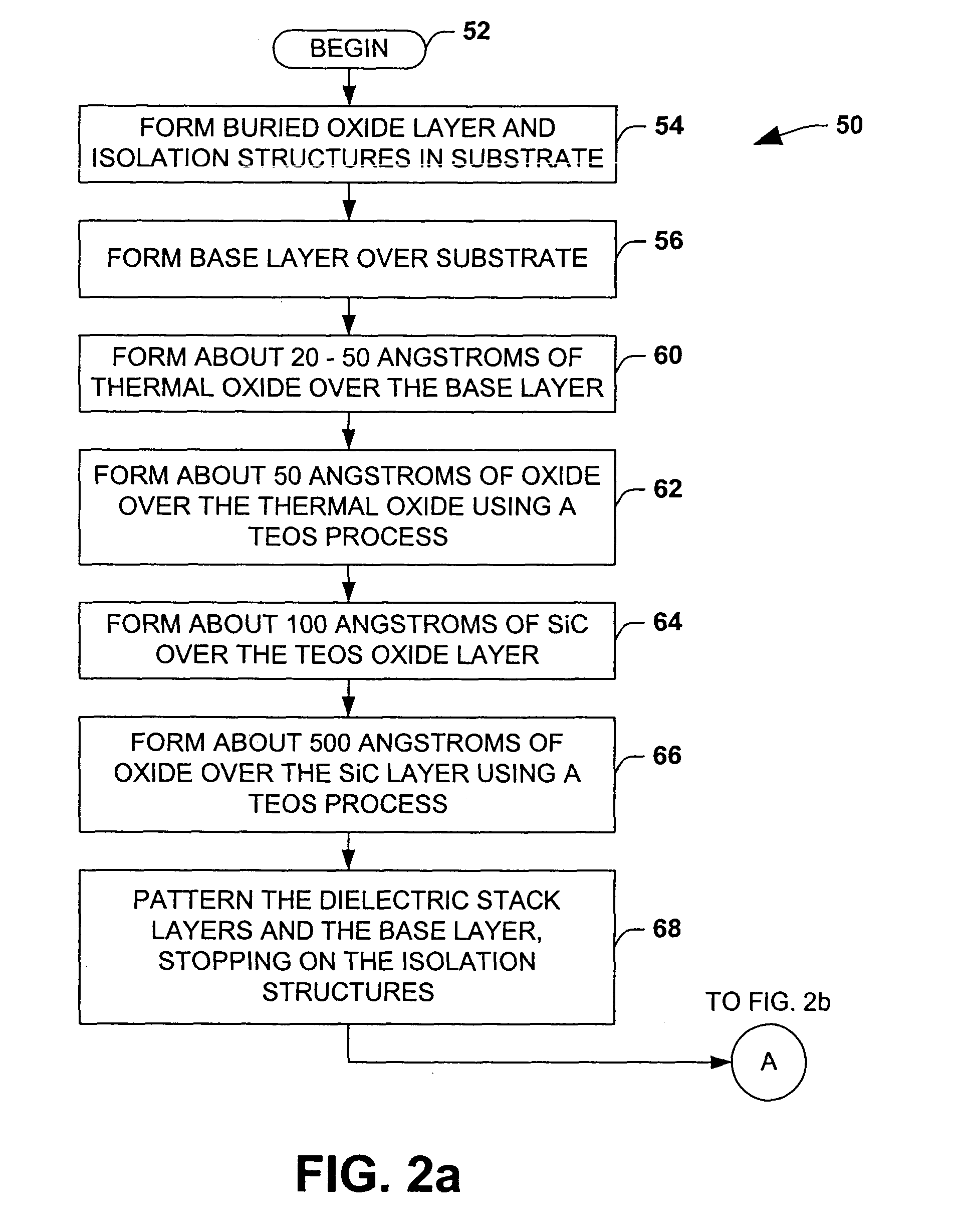
[0040]The present invention addresses these and other problems through use of an amorphous hydrogenated silicon carbide, (a-SiC:H or SiC as an abbreviation) layer in the bipolar emitter-base dielectric stack and appropriate RIE etching in the formation of the emitter-base contact opening. Although illustrated and described below in the context of a particular vertical PNP bipolar transistor architecture, it is to be appreciated that the invention finds application in association with other bipolar designs where polysilicon material is used to form the emitter structure, and that other such applications are deemed as falling within the scope of the present invention and the appended claims. For example, the various aspects of the invention are not limited to bipolar transistors using shallow trench isolation (STI), graded base layer dopant concentrations, buried oxide layers, or the structural dimensions illustrated herein. Moreover, it is noted that the illustrations provided herein...

second preferred embodiment

[0063]In another implementation of the invention, the a-SiC:H layer (e.g., layer 120 of FIGS. 3 and 10-16 above) may be replaced with an a-BC:H layer, or alternatively with any combination of a-SiC:H and a-BC:H. The methodologies of the present invention, such as the above exemplary method 50 of FIGS. 2a and 2b, may be employed to form such a layer, for example, at step 64 of FIG. 2a.

third preferred embodiment

[0064]Alternatively or in combination with the above embodiments and implementations, the upper TEOS oxide layer (e.g., the exemplary layer 116 of FIGS. 3 and 11–16 above) may be removed, wherein the thickness of the carbide layer (e.g. a-SiC:H, or a-BC:H, or combinations thereof, such as layer 120 in the above drawing figures) may be increased to the approximate sum of the original TEOS / carbide thickness.


PUM

PropertyMeasurementUnit
thicknessaaaaaaaaaa
electron currentaaaaaaaaaa
currentaaaaaaaaaa

Abstract

Bipolar transistors and methods for fabricating bipolar transistors are disclosed wherein an emitter-base dielectric stack is formed between emitter and base structures, comprising a carbide layer situated between first and second oxide layers. The carbide layer provides an etch stop for etching the overlying oxide layer, and the underlying oxide layer provides an etch stop for etching the carbide layer to form an emitter-base contact opening.

Description

[0001]This is a divisional application of Ser. No. 10 / 036,763 filed Dec. 21, 2001 now U.S. Pat. No. 6,656,811.FIELD OF INVENTION[0002]The present invention relates generally to semiconductor devices and more particularly to formation of emitter-base junctions for bipolar transistors in a semiconductor device.BACKGROUND OF THE INVENTION[0003]Bipolar transistors are widely employed for switching and amplification of electrical signals in modern semiconductor devices. Such bipolar devices are found in products fabricated using bipolar and BiCMOS processing techniques, which integrates bipolar and CMOS technology. In a BiCMOS device, bipolar transistors are often used for analog signal processing and conditioning, whereas MOS devices are employed for digital signals. NPN bipolar transistors comprise a p-type base situated between an n-type emitter and an n-type collector, whereas PNP type bipolar transistors include an n-type base between a p-type emitter and a p-type collector. Under a...

Claims


Application Information

Patent Timeline
Patent Type & Authority Patents(United States)
IPC IPC(8): H01L27/082H01L27/102H01L29/70H01L31/11H01L21/331H01L21/8249H01L29/24
CPCH01L21/8249H01L29/66272H01L29/66242H01L29/1608
Inventor SWANSON, LELAND S.HOWARD, GREGORY E.
Owner INTEL CORP
Why Eureka
Try Eureka