Method and structures for implementing impedance-controlled coupled noise suppressor for differential interface solder column array

a technology of coupled noise suppression and differential interface solder column array, which is applied in the direction of welding/cutting media/materials, manufacturing tools, and soldering apparatus, etc., can solve the problems of plastic deformation of the solder ball interconnection, fatigue failure of the interconnection between the ceramic substrate and the board, and the actual fatigue life of the bga decreases with increasing the array siz

Inactive Publication Date: 2006-05-02
IBM CORP
View PDF5 Cites 11 Cited by
  • Summary
  • Abstract
  • Description
  • Claims
  • Application Information

AI Technical Summary

Benefits of technology

[0013]In accordance with features of the invention, the impedance-controlled coupled noise suppressor enables the use of long solder columns with minimized coupled noise between adjacent differential pairs of solder columns. The impedance-controlled coupled noise suppressor enables a differential signal pair to propagate together and also return currents flowing in reference planes around the differential signal pair. The impedance-controlled coupled noise suppressor also enables controlled impedance for single signals and minimized coupled noise between adjacent solder columns. An electrical connection is provided between the impedance-controlled coupled noise suppressor structure and an image return current path of the circuit card.

Problems solved by technology

During thermal cycling (on-off cycles), such TCE differences cause plastic deformation of the solder ball interconnections.
Accumulation of plastic strain with repeated thermal cycling ultimately leads to fatigue failure of the interconnections between the ceramic substrate and the board.
The actual fatigue life of a BGA decreases with increasing array size.
A significant disadvantage of the solder column attach over the solder ball attach is the electrical noise coupling between adjacent solder columns.
While the above-identified patent application provides significant improvements over conventional arrangements, additional problems remain.
This results in unwanted coupling between signals that should not have any affinity.
Also, typically when signals pass through a solder column, the signals experience an impedance discontinuity, which can affect the signal quality.
When printed circuit card wiring escapes from modules, the space between the through-vias in the module pin field limit the wireability of the card.

Method used


Image

  • Method and structures for implementing impedance-controlled coupled noise suppressor for differential interface solder column array
  • Method and structures for implementing impedance-controlled coupled noise suppressor for differential interface solder column array
  • Method and structures for implementing impedance-controlled coupled noise suppressor for differential interface solder column array

Examples


Embodiment Construction

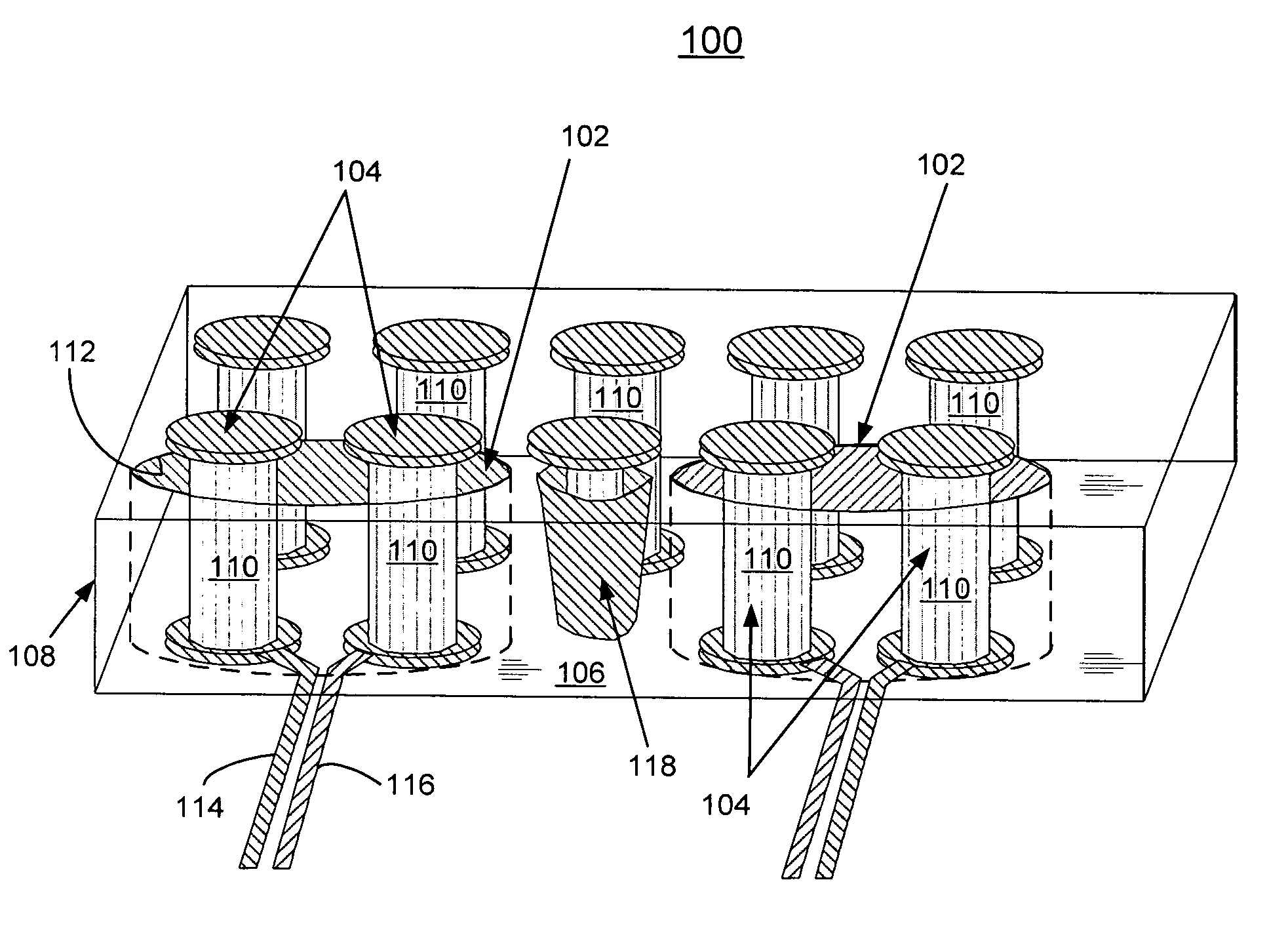
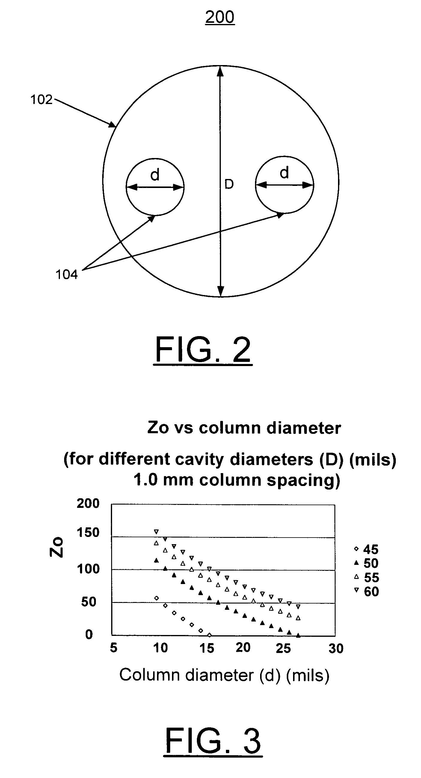
[0025]In accordance with features of the preferred embodiments, a method and structures are provided for implementing impedance-controlled coupled noise suppressor for a differential interface solder column array arranged, for example, as a column grid array (CGA) or in various other array patterns, to make second level solder connections such as for joining a substrate to a circuit card. The impedance-controlled coupled noise suppressor structures of the preferred embodiments enable the use and reliability of longer solder columns, for example, 87 mils (0.087 inch) tall solder columns with substantially comparable electrical advantages of ball grid arrays. The impedance-controlled coupled noise suppressor structures of the preferred embodiments isolate each differential signal pair of solder columns in a solder column package from other solder columns on the package.

[0026]Having reference now to the drawings, in FIG. 1, there is shown an impedance-controlled coupled noise suppresso...


PUM

PropertyMeasurementUnit
diameteraaaaaaaaaa
diameteraaaaaaaaaa
diameteraaaaaaaaaa

Abstract

A method and structures are provided for implementing an impedance-controlled coupled noise suppressor for a differential interface solder column array used to join a substrate to a circuit card. The impedance-controlled coupled noise suppressor structure includes a plurality of elongated through openings that are arranged in a predefined pattern with one or more of the through openings receiving a differential signal pair of solder columns. The elongated through openings have electrically conductive sidewalls and are electrically connected together. The predefined pattern of the elongated, electrically conductive through openings corresponds to a layout of solder columns. The solder columns are attached at opposite ends to a substrate and a circuit card. An electrical connection is provided between the impedance-controlled coupled noise suppressor structure and an image return current path of the circuit card.

Description

FIELD OF THE INVENTION[0001]The present invention relates generally to solder interconnection structures and, more particularly, to a method and structures for implementing impedance-controlled coupled noise suppressor for a differential interface solder column array.DESCRIPTION OF THE RELATED ART[0002]In electronics systems there are various electronic components that require connection to other electronic components or to other levels of packaging. Examples include mounting of integrated circuit chips to a metalized substrate, multilayer ceramic substrate (MLC), laminate organic substrate, glass ceramic substrate, card (direct-chip-attach, DCA), and any substrate made of composite materials meeting thermal and mechanical properties. A second level surface mount technology, such as, a column grid array (CGA) or a ball grid array (BGA) typically is used to form an interconnection between a circuit board and an electronic module assembly such as a chip connected to a MLC.[0003]The te...

Claims


Application Information

Patent Timeline
Patent Type & Authority Patents(United States)
IPC IPC(8): B23K31/02B23K35/12B23K35/14
CPCB23K9/285H05K1/0219H05K3/3436H05K2201/10734H05K2201/09809H05K2201/10424H05K2201/09236
Inventor BARTLEY, GERALD KEITHBECKER, DARRYL JOHNDAHLEN, PAUL ERICGERMANN, PHILIP RAYMONDMAKI, ANDREW B.MAXSON, MARK OWEN
Owner IBM CORP
Why Eureka
Try Eureka