RF amplifier employing active load linearization

Active Publication Date: 2006-05-02
TAHOE RES LTD
View PDF15 Cites 12 Cited by
  • Summary
  • Abstract
  • Description
  • Claims
  • Application Information

AI Technical Summary

Benefits of technology

[0011]In a preferred embodiment of the power amplifier circuit, the second turn-on threshold of the second amplifier device is about 6–10 dB below device saturation of the first amplifier device. The second amplifier device may have a transitional region after the turn-on threshold and a fully turned on region at higher power and the real component of the impedance across the first and second amplifier devices are preferably substantially equal when the second amplifier device is in the fully turned on region. The first and second amplifier devices may be field effect transistors having respective source and gate terminals, and are coupled to receive the input signal applied to their respective gate terminals. The first and second bias circuits are coupled to the respective gate terminals of the first and second amplifier devices and provide first and second fixed voltage bias levels to the respective gate terminals of the first and second amplifier devices to set the respective turn-on thresholds of the first and second amplifier devices. The first and second bias circuits may preferably comprise first and second resistor networks coupled to the DC supply and the respective gate terminals of the first and second amplifier devices. The first and second resistor networks may comprise one or more common resistors. The first and second bias circuits may further comprise first and second low pass matching circuits coupled between the DC supply and the respective gate terminals of the first and second amplifier devices. The power amplifier circuit may further comprise a 90 degree phase inverting circuit coupled between the output load and

Problems solved by technology

In such systems, to preserve signal integrity and prevent transmitter spurious emissions, the amplifying device has to maintain linearity by having sufficient headroom for the signal peaks, albeit producing a modest aver

Method used


Image

  • RF amplifier employing active load linearization
  • RF amplifier employing active load linearization
  • RF amplifier employing active load linearization

Examples


Embodiment Construction

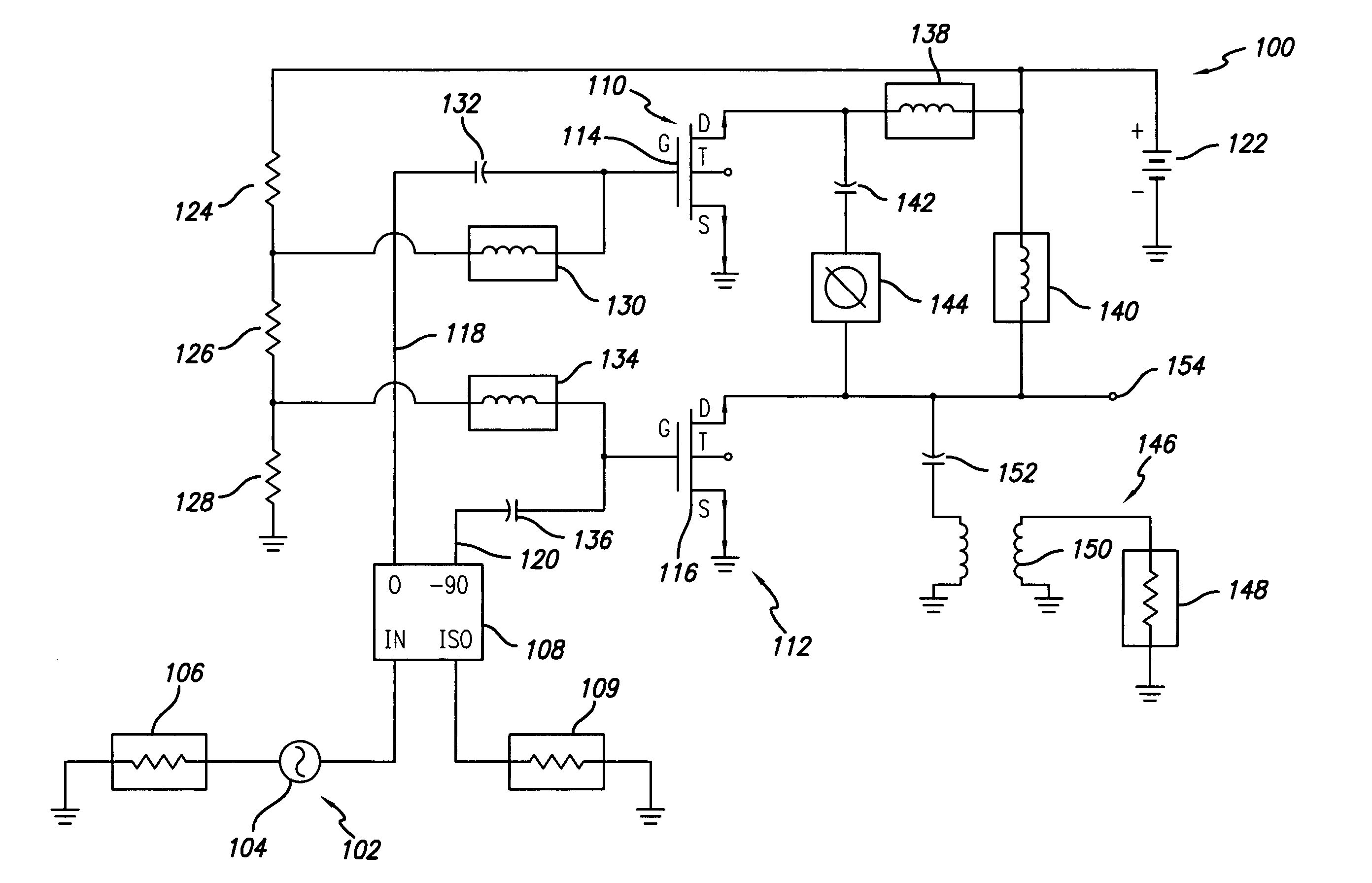
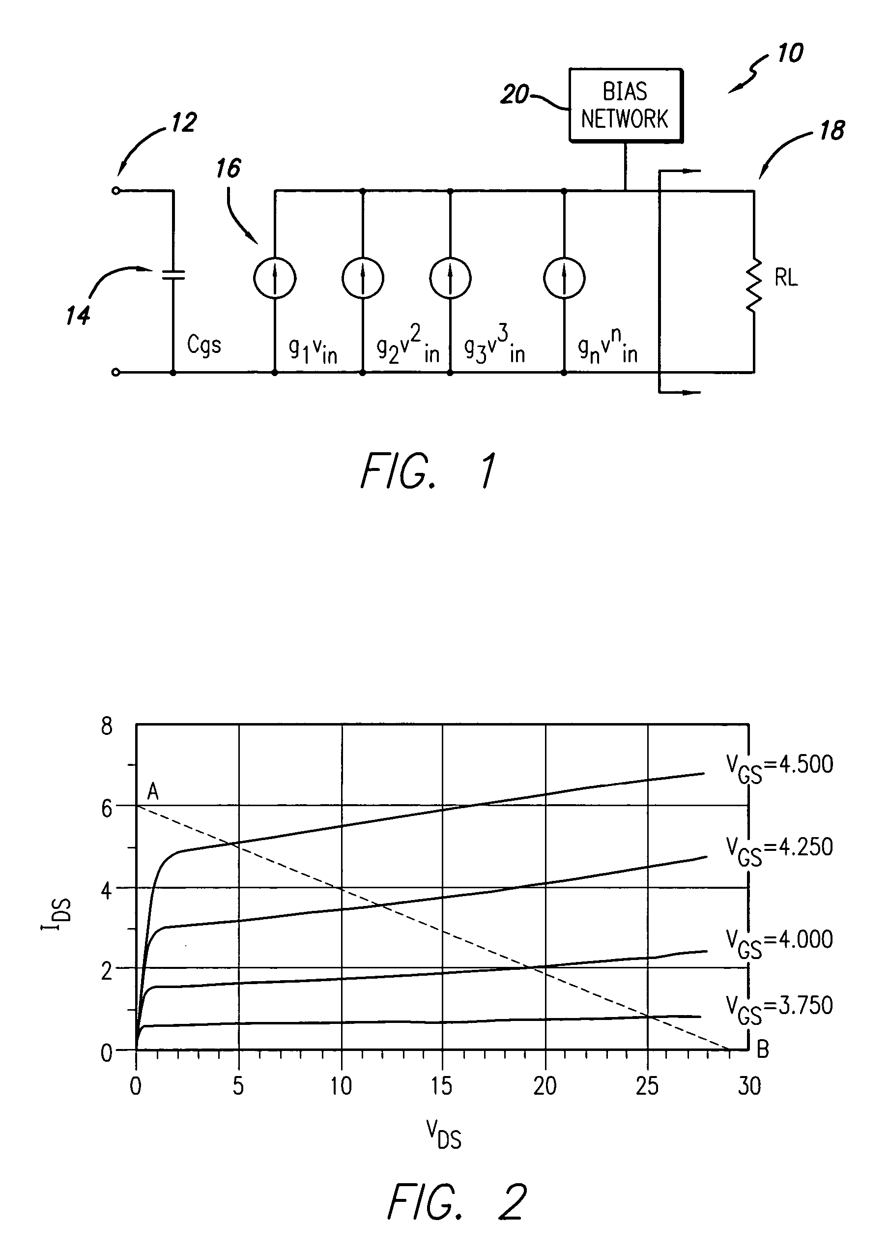
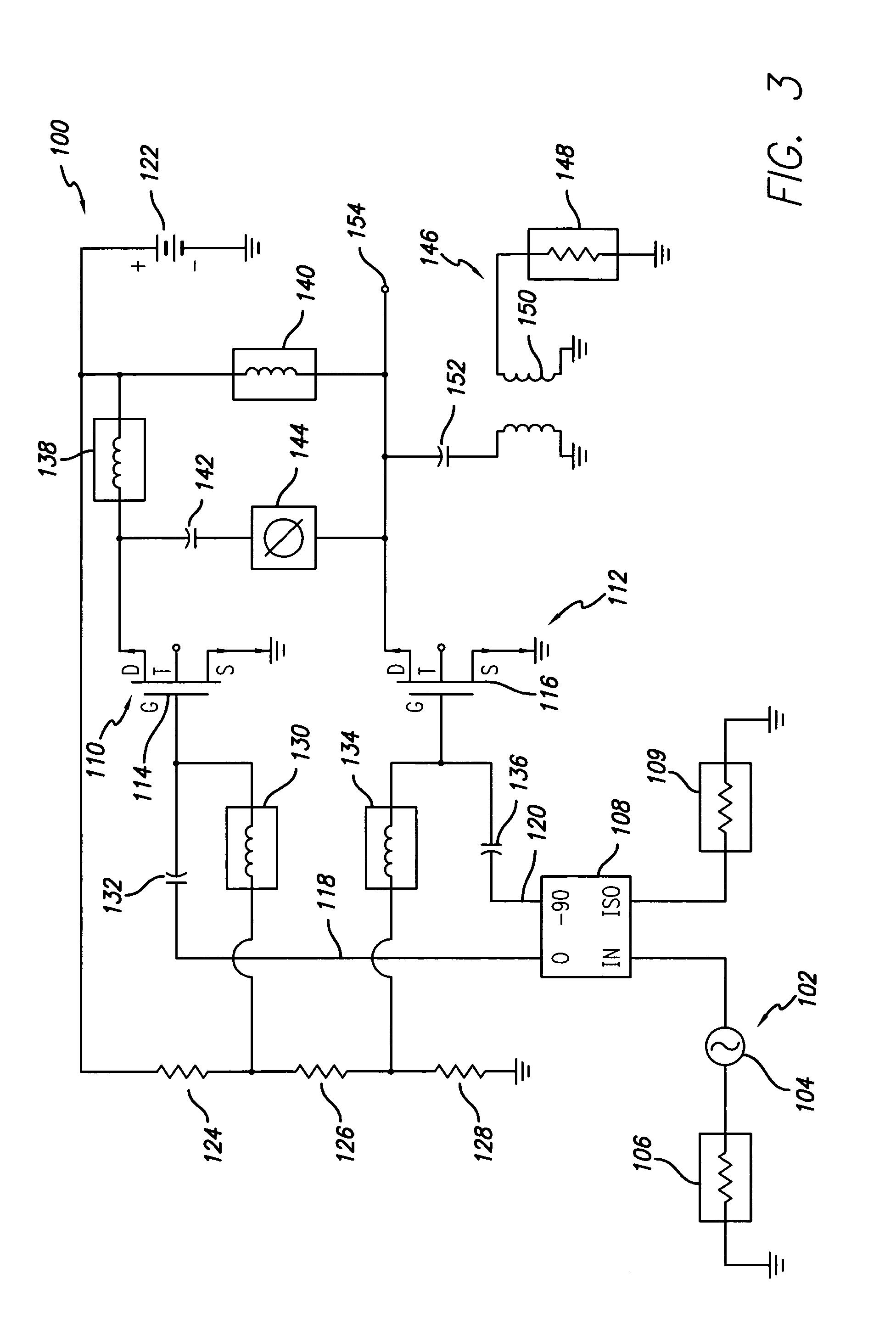
[0023]The present invention provides a linearized high efficiency RF power amplifier and a method for linear amplification of an RF signal. A detailed circuit schematic of a preferred implementation of the amplifier is shown in FIG. 3, described below. First, however, the basic operational characteristics of amplifier devices employed in such circuit will be described in relation to FIG. 1 and FIG. 2.

[0024]The basic structure of a controlled current source as embedded in an amplifier circuit 10 is shown in FIG. 1. This structure is a representation of a voltage controlled current source and is a simplified representation of solid-state devices such as a Field Effect Transistor (FET). The mechanisms responsible for the active device (transistor) nonlinearity are multifold. The device transconductance, the input and the output nonlinearities, all contribute to the amplifier distortion and are well known to those skilled in the art. The following description of the invention is equally...


PUM


Abstract

A method and apparatus for linear amplification of a modulated carrier signal or multi-carrier signal is disclosed. The linearity of the amplifier is improved by employing dynamic load line adjustments. A second current source coupled to the amplifier output load is turned on just before the amplifier reaches a nonlinear regime and reduces the effective load to prevent the amplifier allowing sufficient power to reach the nonlinear regime near saturation. The technique is particularly advantageous for amplification of a signal with large peak to average ratio.

Description

RELATED APPLICATION INFORMATION[0001]The present application claims priority under 35 USC 119(e) of provisional application Ser. No. 60 / 468,309 filed May 6, 2003, the disclosure of which is incorporated herein by reference in its entirety.BACKGROUND OF THE INVENTION[0002]1. Field of the Invention[0003]The present invention is related to radio frequency (RF) amplifiers. More particularly, the present invention is related to radio frequency power amplifiers used in wireless communication applications such as cellular base stations where signals with high peak to average ratios are generated and amplified.[0004]2. Description of the Prior Art and Related Background Information[0005]Most digitally modulated carrier signals used in modern telecommunication systems have an amplitude envelope showing a large peak to average ratio. In such systems, to preserve signal integrity and prevent transmitter spurious emissions, the amplifying device has to maintain linearity by having sufficient he...

Claims


Application Information

Patent Timeline
IPC IPC(8): H03F1/14H03F1/02H03F1/32H03F3/60
CPCH03F1/0205H03F1/0288H03F1/3205H03F3/602H03F2200/198
Inventor KHANIFAR, AHMADMASLENNIKOV, NIKOLAI
Owner TAHOE RES LTD
Why Eureka
Try Eureka