Technology dependent transformations for Silicon-On-Insulator in digital design synthesis

a technology of digital design and transformation, applied in the field of technology dependent transformations for digital design synthesis, can solve the problems of reducing the realistic affecting the overall quality of the design, and unable to meet timing, size or power., and achieves the effect of reducing cross-coupling, realizing the improvement of such an approach, and reducing interconnected delay

Inactive Publication Date: 2006-05-02
RANA AMAR PAL SINGH +1
View PDF6 Cites 20 Cited by
  • Summary
  • Abstract
  • Description
  • Claims
  • Application Information

AI Technical Summary

Benefits of technology

[0037]The patent application 20020053063 Bhattacharya, Debashis et. al utilizes automated dynamic transistor level design where gate approach does not meet timing constraints in CMOS ASIC design. The realistic improvement of such an approach is considerably diminished in each of the automated steps for not being fully capable to match the manual optimizations due to algorithmic deficiencies, unacceptable CPU run time and memory needed during: the input design specification technology independent logic minimization stage, transistor level stages clustering, transistor sizing algorithms, local automated dynamic precharge and evaluation clock generation at the high frequencies needed and automated layout of dynamic clusters and subsequent placement and routing of such dynamic clusters having widely differing aspect ratios with the rest of standard cells for CMOS ASIC design resulting in overall questionable improvement to meet timing, size or power constraints. With lower dielectric material between the interconnects, cross-coupling is lowered resulting in lower interconnected delay, diminishing the need of automated gate sizing as taught in U.S. Pat. No. 6,253,361 of Buch, Premal and eliminating the need for automated CMOS transistor level design as taught in patent application 20020053063 to automatically substitute for weak portions of gate design flow.

Problems solved by technology

The realistic improvement of such an approach is considerably diminished in each of the automated steps for not being fully capable to match the manual optimizations due to algorithmic deficiencies, unacceptable CPU run time and memory needed during: the input design specification technology independent logic minimization stage, transistor level stages clustering, transistor sizing algorithms, local automated dynamic precharge and evaluation clock generation at the high frequencies needed and automated layout of dynamic clusters and subsequent placement and routing of such dynamic clusters having widely differing aspect ratios with the rest of standard cells for CMOS ASIC design resulting in overall questionable improvement to meet timing, size or power constraints.

Method used


Image

  • Technology dependent transformations for Silicon-On-Insulator in digital design synthesis
  • Technology dependent transformations for Silicon-On-Insulator in digital design synthesis
  • Technology dependent transformations for Silicon-On-Insulator in digital design synthesis

Examples


Embodiment Construction

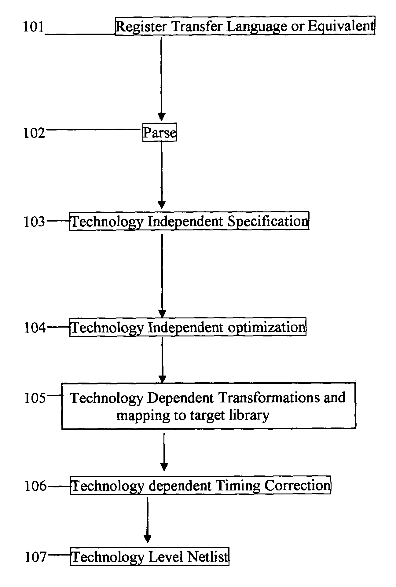
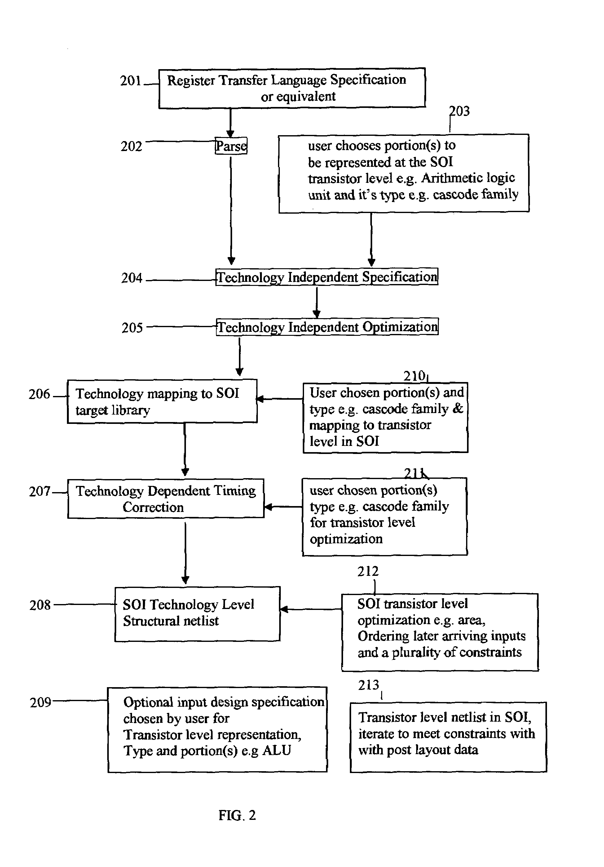
[0047]The present invention pertains to automated technology dependent transformations in Silicon-On-Insulator (SOI) during the digital design synthesis, the transformations include the steps of receiving input design specification in the form of technology independent specification or interconnected structural blocks, where the structural blocks have been described as a library of standard-cells; performing the technology dependent transformations during the digital design synthesis, resulting in interconnected SOI standard-cells from a SOI target library accounting for floating body effects, including floating body effects affecting delays over long periods of simulation time or testing over long times on fabricated SOI library cells, or SOI transistor level representations or a combination thereof, transistor sizing and evaluating the standard-cell mapping or transistor-level representation for all or portion of the input design specification iteratively to meet delay and power c...


PUM


Abstract

The present invention pertains to automated technology dependent transformations for Silicon-On-Insulator (SOI) in the digital design synthesis, the transformations include the steps of receiving input design specification in the form of technology independent specification or interconnected library of standard-cells; performing the technology dependent transformations in the digital design synthesis, resulting in interconnected SOI standard-cells from a SOI target library accounting for floating body effects, including floating body effects affecting delays over long periods of simulation time or testing over long times on fabricated SOI library cells, or SOI transistor level representations, transistor sizing and evaluating the standard-cell mapping and transistor-level representation for all or portion of the input design specification iteratively to meet delay and power constraints for SOI.

Description

BACKGROUND OF THE INVENTION[0001]1. Technical Field[0002]The invention relates to technology dependent transformations for design automation and more particularly to technology dependent CMOS transistor level transformations where user specifies the portion or portions to be represented at the transistor level and the transistor level type e.g. cascode family, NORA logic etc. It also relates to SOI gate or transistor-level synthesis.[0003]2. Glossary of Terms[0004]A cluster is the single organizational component of a logic synthesis database. It has input and output terminals, which allow connection to other clusters by nets. Each cluster is designated by a technology type e.g. CMOS push pull cascode family or SOI dynamic pre-charge evaluation logic, which may be a primitive or may reference a definition in terms of other clusters. Thus, a hierarchy of clusters can be used and an instance of a high-level cluster type, may be treated as a single cluster or expanded. These clusters ar...

Claims


Application Information

Patent Timeline
Patent Type & Authority Patents(United States)
IPC IPC(8): G06F17/50
CPCG06F17/5045G06F30/30
Inventor RANA, AMAR PAL SINGHSINGH, NIRMAL
Owner RANA AMAR PAL SINGH
Why Eureka
Try Eureka