Semiconductor device with polymer insulation of some electrodes

Inactive Publication Date: 2006-05-09
MITSUBISHI ELECTRIC CORP
View PDF3 Cites 0 Cited by
  • Summary
  • Abstract
  • Description
  • Claims
  • Application Information

AI Technical Summary

Benefits of technology

[0012]The present invention has been made to solve the above problem, and has its object to provide a semiconductor device which can simplify the structure of the semiconductor device to easily realize the facility of the manufacturing process. It is another object of the present invention to provide a semiconductor device which can suppresses the occurrence of camber in a die-bonding process for a semiconductor chip.
[0018]According to the present invention, unlike a prior art, since via holes need not be formed in a semiconductor substrate unlike a conventional semiconductor substrate, a semiconductor chip structure can be simplified, and the chip manufacturing process can be simplified. Furthermore, according to the present invention, since camber in a die-bonding process for the semiconductor device can be reduced, an AuSn solder between a heat sink on the back plane of the chip and a package is uniformly formed to have a small thickness, and the heat resistance of the device can be reduced.

Problems solved by technology

Hence, every gate pad 2 must be wire-bonded and therefore the assembly process become complex and the characteristics caused by variation of wire-bonding lengths is degraded.
In addition, as shown in FIG. 16, when a semiconductor chip is die-bonded to the substrate of a package by an AuSn solder in assembly of a device, camber occurs due to a difference of thermal expansions between the semiconductor substrate 1 and the back plane heat sink 10, the thickness of solder on each end of the semiconductor chip increases, and the heat resistance of the device disadvantageously increases.

Method used


Image

  • Semiconductor device with polymer insulation of some electrodes
  • Semiconductor device with polymer insulation of some electrodes
  • Semiconductor device with polymer insulation of some electrodes

Examples


first embodiment

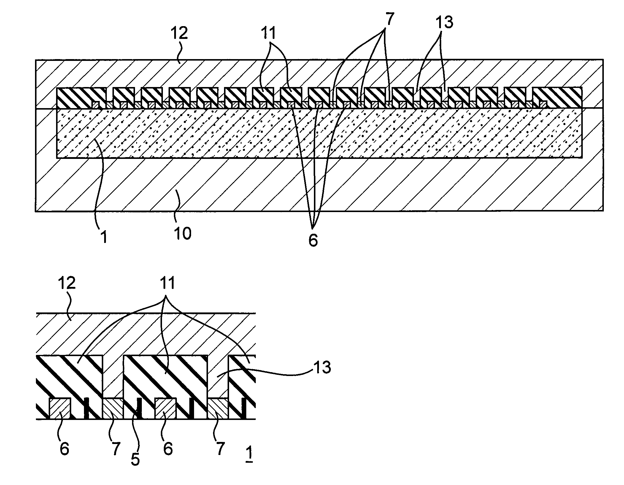
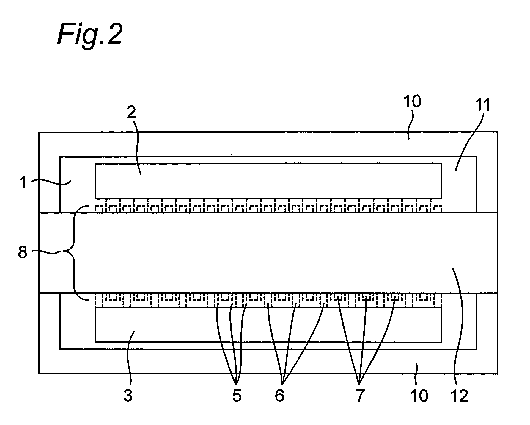
[0037]A semiconductor device according to the present invention has a plurality of field effect transistors (FETs) formed thereon. FIG. 1A is a sectional side view showing the structure of the semiconductor device according to the present invention. FIG. 1B is a partially enlarged view of a section of the semiconductor device. FIG. 2 is a top view showing the structure of the semiconductor device of the present invention.

[0038]As shown in FIGS. 1 and 2, gate electrodes 5 serving as control electrodes of FETs and drain electrodes 6 and source electrodes 7 serving as main electrodes of the FETs are arranged on a semiconductor substrate 1. The drain electrodes 6 and the source electrodes 7 are alternately arranged, and the gate electrodes 5 are arranged between the electrodes 6 and 7. It should be noted that in FIG. 1A the gate electrodes 5 are omitted for the sake of visual convenience (as well as FIG. 8, FIG. 11, and the like). In FIG. 1B, a partially enlarged view of the section of ...

second embodiment

[0045]A semiconductor device according to another embodiment of the present invention will be described below with reference to FIGS. 3 to 6. FIG. 3 shows a layout pattern obtained when the semiconductor device of this embodiment is viewed from the top. FIG. 4 shows a layout pattern obtained when the semiconductor device is viewed from the bottom. FIG. 5 is a sectional view of the semiconductor device cut along V—V line in FIG. 3. FIG. 6 is a sectional view of the semiconductor device cut along VI—VI line in FIG. 3.

[0046]In this embodiment, as in the first embodiment, as shown in FIG. 5, source electrodes 7 formed on a semiconductor substrate 1 are connected to a chip surface ground electrode 12 through support sections 13, so that the same effect as that of the first embodiment can be obtained.

[0047]As shown in FIG. 3, gate and drain pads 2 and 3 are provided on the semiconductor substrate 1. The gate and drain pads 2 and 3 are not only formed on the front plane of the semiconducto...

third embodiment

[0052]In this embodiment, a semiconductor device which can prevent camber in a die-bonding process will be described below with reference to FIGS. 7 and 8. FIG. 7 shows a layout pattern of the semiconductor device according to this embodiment. FIG. 8 is a sectional side view of the semiconductor device. As shown in FIG. 8, in this embodiment, a protecting film 11a which is made of polymer material with a low dielectric constant is formed on a principal plane on which electrodes 5, 6 and 7 on a semiconductor substrate 1 are formed.

[0053]Hence, since the protecting film 11a made of the low-dielectric-constant polymer material is formed, it becomes possible to press the front plane of the chip by a chip handling collet 16 or the like in a die-bonding process as shown in FIG. 9 so that camber occurring in a die-bonding process can be reduced. Due to the reduction in camber, an AuSn solder between a heat sink 10 and a package 15 on the back plane of the chip is uniformly formed to have a...


PUM


Abstract

A semiconductor device includes a semiconductor substrate having a principal plane on which gate, source, and drain electrodes are located. A film made of a polymer with a low dielectric constant is over the gate and drain electrodes to insulate the gate and drain electrodes from the source electrodes. A chip surface electrode located over the low-dielectric-constant polymer film and the source electrode, and connected to ground potential. The source electrode is provided with the ground potential through the chip surface electrode.

Description

BACKGROUND OF THE INVENTION[0001]1. Field of the Invention[0002]The present invention relates to a semiconductor device including transistors, each transistor having a plurality of electrodes.[0003]2. Description of the Background Art[0004]FIG. 14 is a plan view of a conventional semiconductor chip on which a plurality of field effect transistors (FETs) are formed, and shows an electrode arrangement of FETs formed on the semiconductor chip. FIG. 15 is a sectional view of the semiconductor chip when viewed from the side.[0005]As shown in FIG. 14, gate electrodes 5, drain electrodes 6 and source electrodes 7 of FETs are arranged on a semiconductor substrate 1. The gate electrode 5, drain electrode 6 and source electrode 7 are connected to a gate pad 2, drain pad 3 and source pad 4, respectively. The gate pad 2 and source pad 4 are alternately arranged as shown in FIG. 14. A via hole 9 is formed in the source pad 4.[0006]As shown in FIG. 15, the via hole 9 is formed in the semiconducto...

Claims


Application Information

Patent Timeline
IPC IPC(8): H01L29/76H01L29/94H01L29/417H01L23/31H01L23/367H01L23/48H01L23/482H01L25/07H01L25/18
CPCH01L23/3171H01L23/3677H01L23/4824H01L2924/12044H01L2924/0002H01L2924/3511H01L2924/00
Inventor KUNII, TETSUOHATTORI, RYOKAWATA, HIROSHI
Owner MITSUBISHI ELECTRIC CORP
Why Eureka
Try Eureka