Voltage isolation buffer with AC coupled and DC coupled hall effect magnetic field sensors

a technology of hall effect magnetic field sensor and voltage isolation buffer, which is applied in the direction of liquid/fluent solid measurement, instruments, and converting sensor output using wave/particle radiation, etc., and can solve the problems of silicon based hall effect sensor performance suffers

Inactive Publication Date: 2006-05-09
OL SECURITY LIABILITY CO
View PDF17 Cites 17 Cited by
  • Summary
  • Abstract
  • Description
  • Claims
  • Application Information

AI Technical Summary

Problems solved by technology

However, these patents fail to address the problem that, in general, the performance of silicon based Hall effect sensors suffers due to large variations in magnetic field sensitivities and variations in DC-offset due to temperature changes.

Method used


Image

  • Voltage isolation buffer with AC coupled and DC coupled hall effect magnetic field sensors
  • Voltage isolation buffer with AC coupled and DC coupled hall effect magnetic field sensors
  • Voltage isolation buffer with AC coupled and DC coupled hall effect magnetic field sensors

Examples


Embodiment Construction

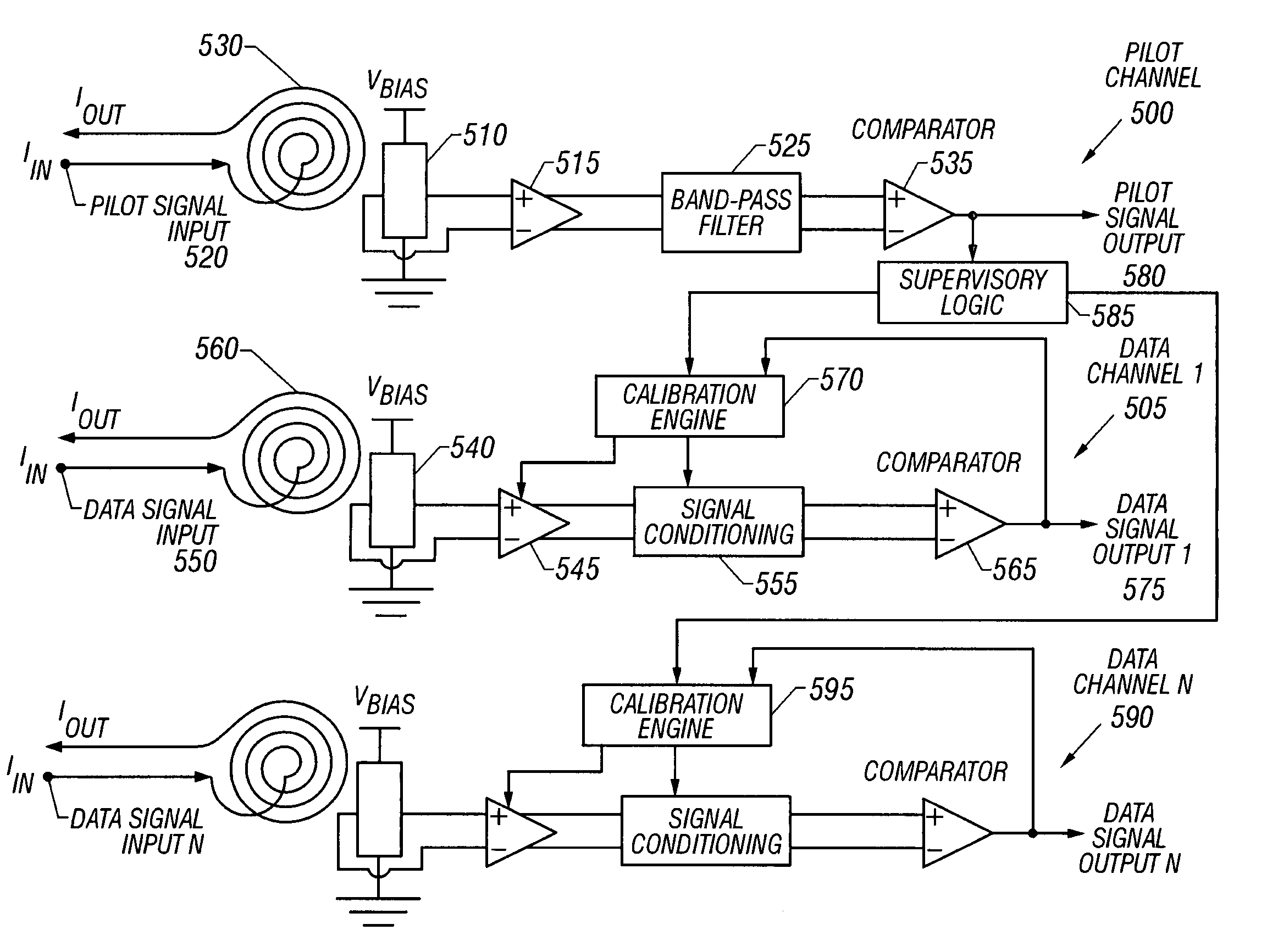
[0026]The following invention addresses the shortcomings of the prior art associated with the temperature related effects of a Hall effect voltage isolation barrier. In particular, a variation in the magnetic field signal is sensed with a Hall effect magnetic field sensor which produces an electrical signal proportional to the magnetic field.

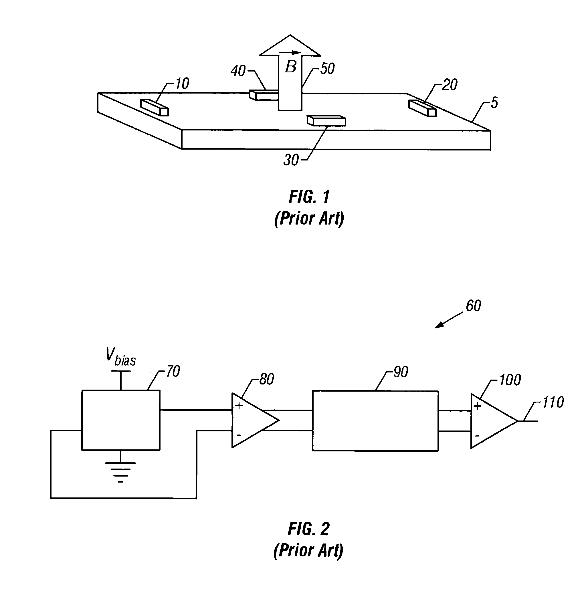
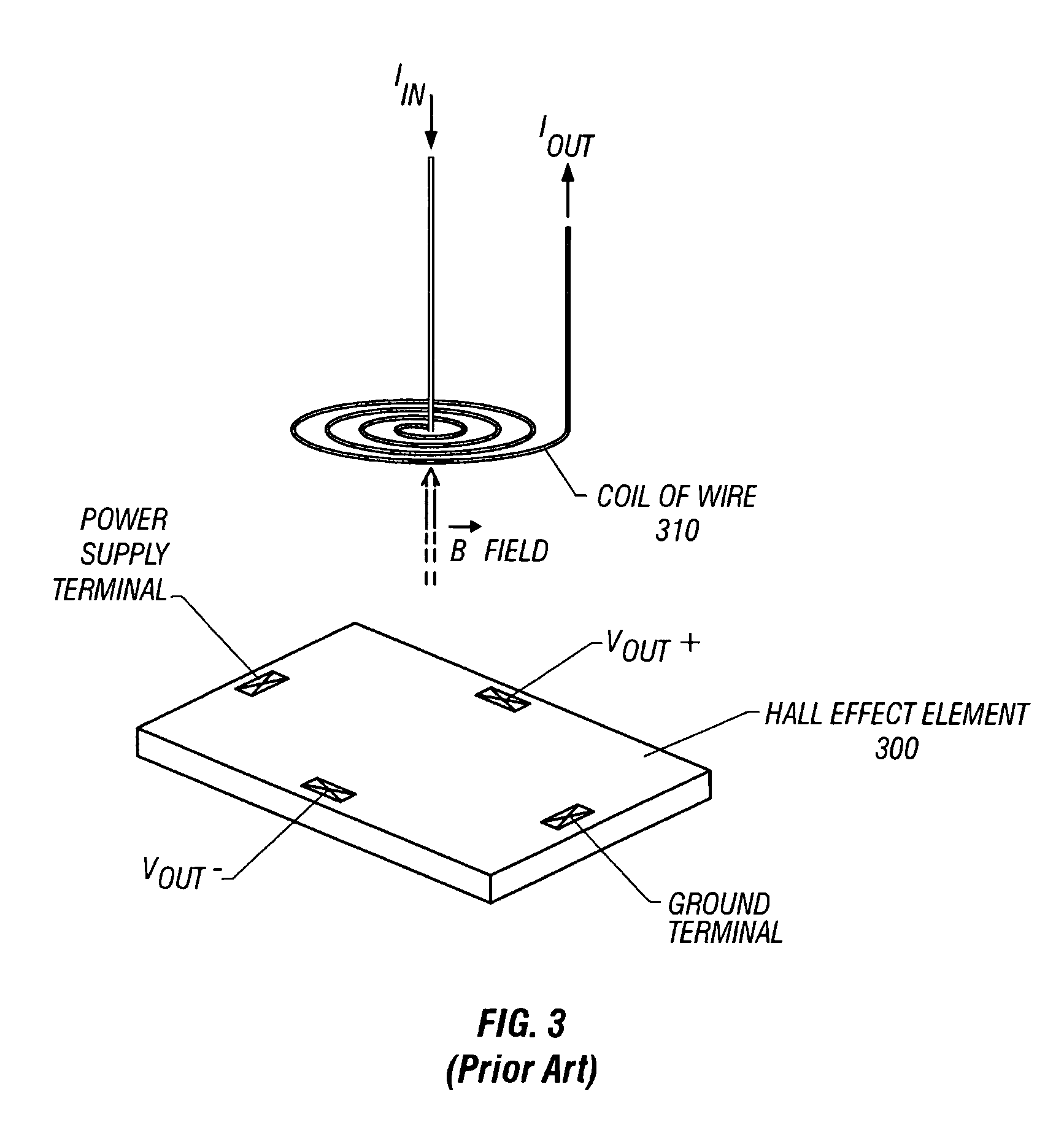
[0027]FIG. 1 depicts a block diagram of a prior art Hall effect element 5. Hall effect element 5 includes power supply terminals 10 and 20 and signal terminals 30 and 40. A bias voltage is applied across power supply terminals 10 and 20. The voltage difference across signal terminals 30 and 40 is given from the following:

[0028]VH=VS·μ·B·(k·(w / l))+Voffset;Eq.⁢1

and is proportional to the magnetic field 50 that is perpendicular to the top surface of Hall effect element 5. With respect to Equation 1, VH is the voltage across signal terminals 30 and 40, VS is the voltage across power terminals 10 and 20, μ is the mobility of the semiconductor materia...


PUM


Abstract

A voltage isolation buffer, including a pilot channel having a first Hall effect element and a data channel having a second Hall effect element is disclosed. The pilot channel is preferably AC coupled, and the data channel is preferably DC coupled. The voltage isolation buffer may include a calibration engine, which may be configurable to calibrate the voltage generated by the second Hall effect element based on the information from the first Hall effect element. A bi-directional voltage isolation buffer is also disclosed, including a first integrated circuit and a second integrated circuit. The first integrated circuit includes a DC coupled Hall effect sensor and an AC coupled Hall effect sensor. The second integrated circuit includes an AC coupled Hall effect sensor and a DC coupled Hall effect sensor. A method for transmitting data across a voltage isolation barrier is also disclosed including the steps of generating a first hall voltage signal, AC coupling the first Hall voltage signal, generating a second Hall voltage signal, DC coupling the second Hall voltage signal, and calibrating the second Hall voltage signal, wherein the step of calibrating is controlled by the first Hall voltage signal.

Description

CROSS-REFERENCE TO RELATED APPLICATIONS[0001]This application is a divisional application of U.S. application Ser. No. 10 / 076,951 filed on Feb. 15, 2002 U.S. Pat. No. 6,879,145. The benefit of 35 U.S.C. § 120 is hereby claimed for the above-referenced application. The contents of application Ser. No. 10 / 076,951 are hereby incorporated by reference.BACKGROUND OF THE INVENTION[0002]1. Field of the Invention[0003]The present invention relates to voltage isolation barriers, and in particular, to solid-state voltage isolation buffers which allow information to be transmitted across the voltage isolation barrier via a magnetic field.[0004]2. Description of Related Art[0005]Many electronic systems, such as industrial control systems, require some form of electrical isolation in order to protect circuits from large voltage spikes. A benefit to electrical isolation is the avoidance of ground loops that significantly increase system noise. Other benefits are related to protecting people from ...

Claims


Application Information

Patent Timeline
Patent Type & Authority Patents(United States)
IPC IPC(8): G01R31/00G01D3/08G01D5/48G01D18/00
CPCG01D3/08G01D21/00G01D18/006
Inventor HARRIS, LARRY L.
Owner OL SECURITY LIABILITY CO
Why Eureka
Try Eureka