Return-to-zero current switching digital-to-analog converter

a digital-to-analog converter and zero current technology, applied in the field of digital-to-analog converters, can solve the problems of significant noise in the actual dac output, significant limit the use of the dac in high frequency applications, unacceptable level of distortion in the dac output, etc., and achieve the effect of reducing switching and clock-induced noise and extending the frequency rang

Inactive Publication Date: 2006-05-09
OTROSANI ASSET MGMT L L C
View PDF8 Cites 37 Cited by
  • Summary
  • Abstract
  • Description
  • Claims
  • Application Information

AI Technical Summary

Benefits of technology

[0013]A “return-to-zero” (RZ) current switching DAC is presented which overcomes the problems noted above, reducing switching- and clock-induced noise and extending the frequency range over which the DAC may be used.
[0015]The present DAC includes a plurality of “return-to-zero” (RZ) circuits, connected between respective intermediate nodes and single or differential analog output nodes. Each RZ circuit comprises a first transistor connected between the intermediate node and an analog output node and driven with a fixed bias voltage Vbias, and a second transistor connected between the intermediate node and a fixed voltage (preferably ground) and driven with a control signal. When the DAC operates in RZ mode, the control signal is arranged to toggle above and below Vbias in synchronization with the CK signal. Thus, when the control signal toggles below Vbias, the first transistor turns on and directs current source current to an analog output node, and when the control signal toggles above Vbias, the second transistor turns on and directs the current source current to the fixed voltage. Current conducted by the first transistor is coupled to an analog output node via an output network, typically a R-2R ladder network, which is connected to the analog output node and arranged such that the analog output voltage is pulled to the “zero” potential when the currents applied to the intermediate nodes are directed to the fixed voltage via the RZ circuits. When so arranged, the RZ circuits prevent switching noise that arises when clock signal CK is asserted and the control signals change state from appearing on the analog output node. In addition, because each RZ circuits' first transistor is not clocked, clock noise that might otherwise be coupled to the analog output nodes is substantially reduced.

Problems solved by technology

As can be seen, the actual DAC output exhibits a considerable amount of noise; this is caused by switching slew and glitches which arise when the control signals change state, disconnecting some current sources from the analog output lines and connecting others.
This non-linear source of error can result in an unacceptable level of distortion in the DAC output.
This attenuation can necessitate the use of a correction filter, and can significantly limit the DAC's use in high frequency applications.
However, this approach also has drawbacks.

Method used


Image

  • Return-to-zero current switching digital-to-analog converter
  • Return-to-zero current switching digital-to-analog converter
  • Return-to-zero current switching digital-to-analog converter

Examples


Embodiment Construction

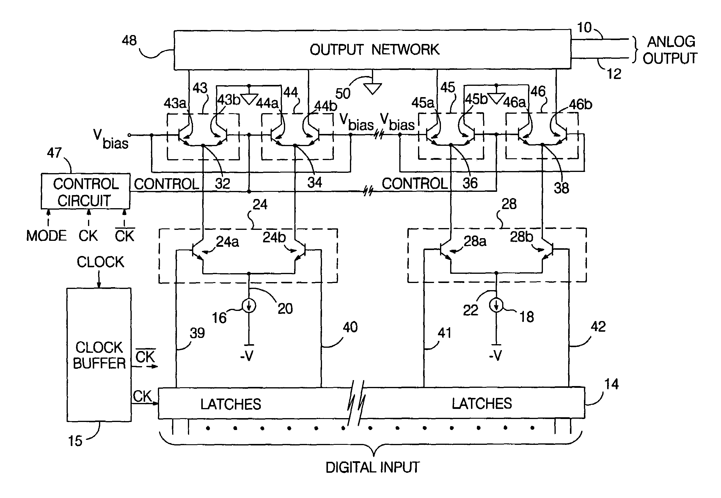
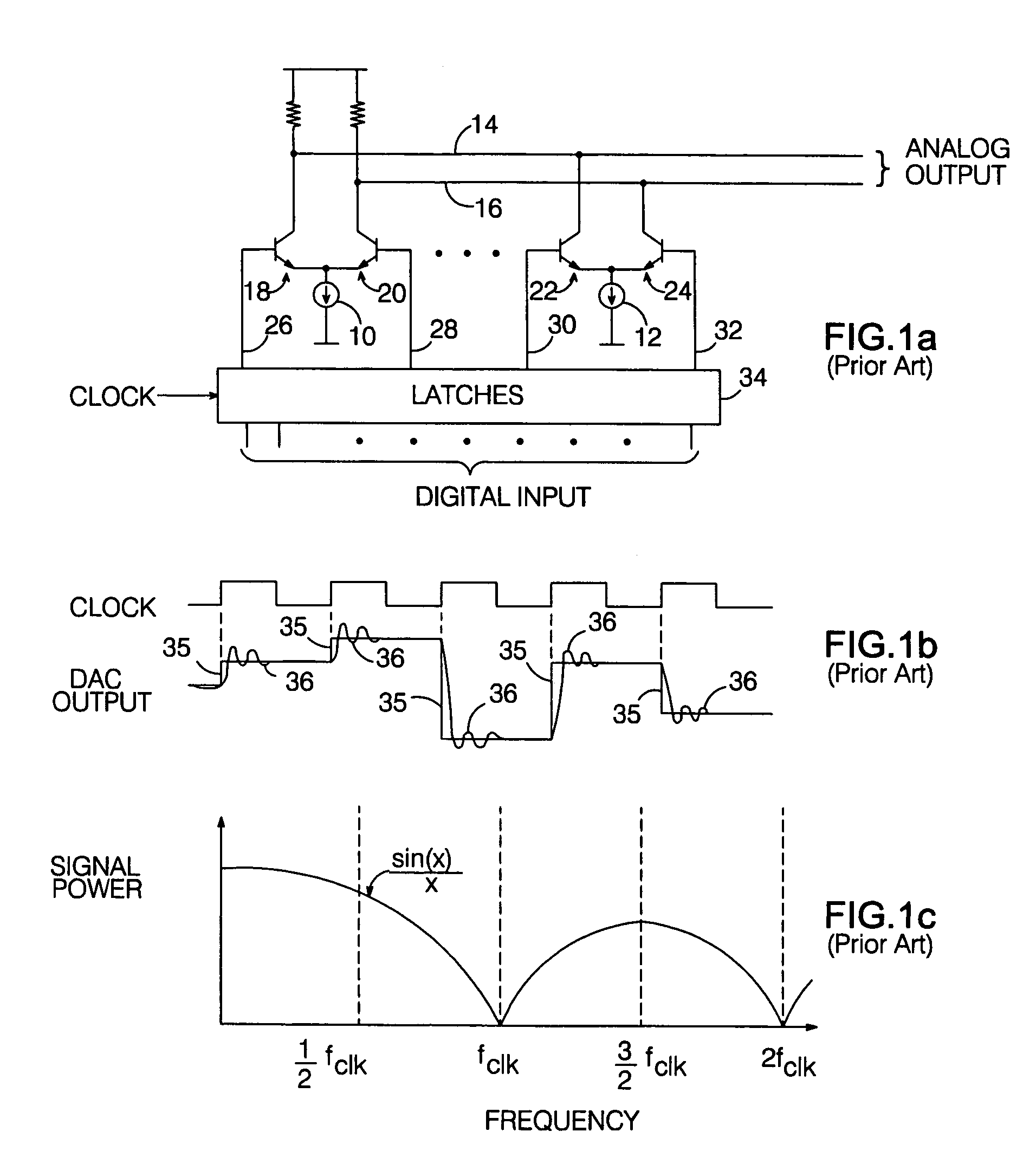
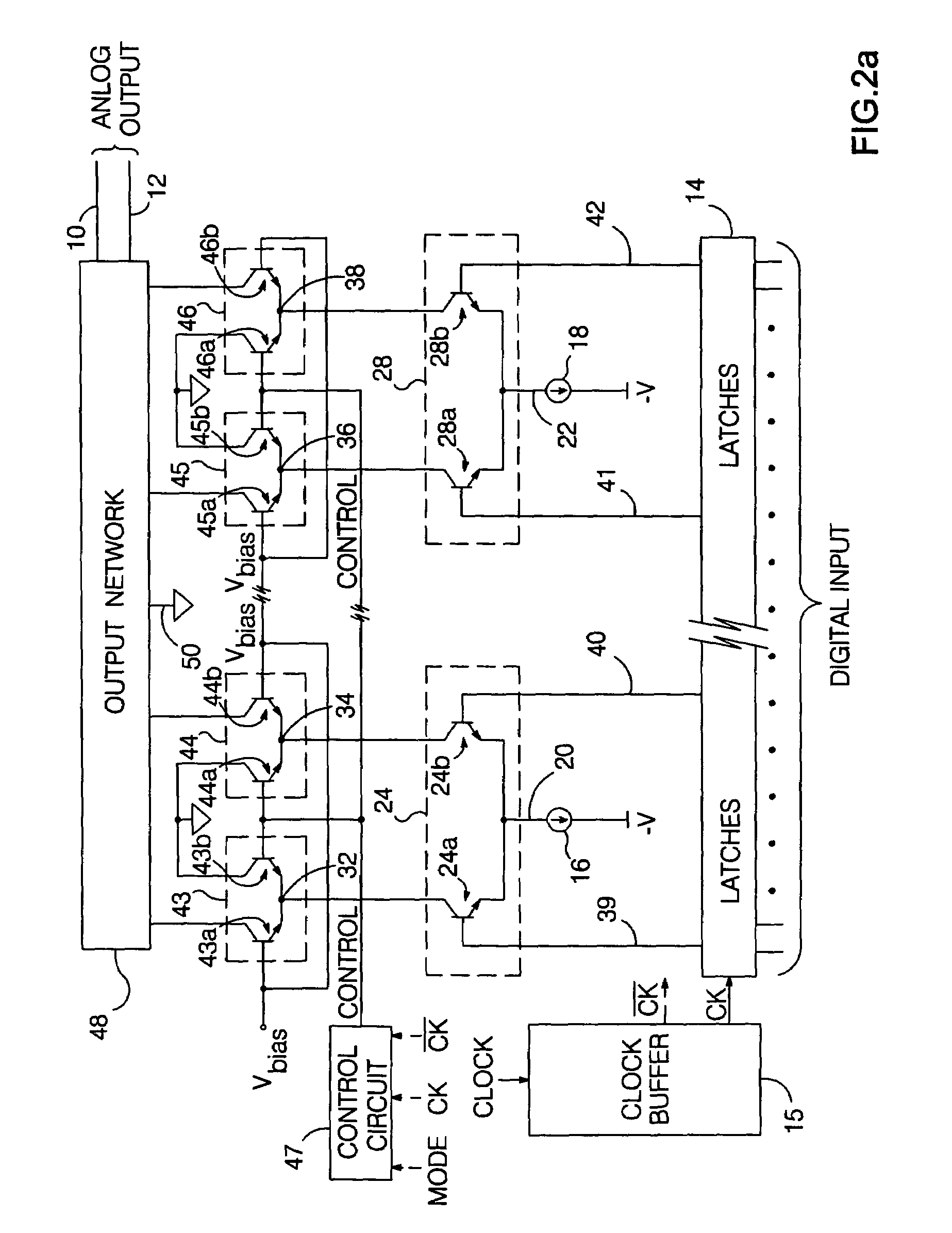
[0033]An RZ current switching DAC per the present invention is shown in FIG. 2a. The DAC receives a digital input word and provides an analog output voltage. In the exemplary embodiment shown in FIG. 2a, the DAC provides a differential output on first and second analog output lines 10 and 12. A “zero” potential, which could be ground or a non-zero potential, is pre-defined for the DAC's analog output lines. The digital input word is received by clocked circuitry 14, typically a set of latches. The DAC typically includes a clock buffer 15, which receives a clock signal CLOCK, and provides a first clock signal CK and a second clock signal {overscore (CK )} which is the inverse of CK. The DAC includes a plurality of current sources; only two current sources (16, 18) are shown in FIG. 2a, but a practical DAC would typically include 10 or more current sources. Current sources 16 and 18 have respective outputs 20 and 22.

[0034]In the differential embodiment shown, the current source output...


PUM


Abstract

A “return-to-zero” (RZ) current switching DAC includes an analog output node for which a “zero” potential has been defined. The outputs of a plurality of current sources are selectively directed to respective intermediate nodes in response to respective control signals, which are varied in synchronization with a clock signal CK. A plurality of RZ circuits are connected between respective intermediate nodes and the analog output node. In a preferred embodiment, each RZ circuit directs the current applied to a respective intermediate node to ground or to the analog output node in synchronization with CK. An output network pulls the analog output node to the “zero” potential when currents applied to the intermediate nodes are directed to ground.

Description

[0001]This application claims the benefit of provisional patent application No. 60 / 592,420 to Choe, filed Jul. 30, 2004.BACKGROUND OF THE INVENTION[0002]1. Field of the Invention[0003]This invention relates to the field of digital-to-analog converters (DACs), and particularly to techniques for reducing switching noise in current switching DACs.[0004]2. Description of the Related Art[0005]A basic current switching DAC is shown in FIG. 1a. A plurality of current sources 10, 12 are connected to a analog output lines 14, 16 via pairs of switches 18, 20 and 22, 24. The switches are typically implemented with transistors, which are controlled using respective control signals 26, 28, 30, 32 provided by a latch circuit 34. Latch circuit 34 receives a digital input word via a set of input lines, as well as a clock signal.[0006]The digital input word represents a desired analog output voltage. In operation, latch circuit 34 responds to an applied digital input word by setting control signals ...

Claims


Application Information

Patent Timeline
Patent Type & Authority Patents(United States)
IPC IPC(8): H03M1/66
CPCH03M1/0881H03M1/785
Inventor CHOE, MYUNG-JUN
Owner OTROSANI ASSET MGMT L L C
Why Eureka
Try Eureka