Layout for a semiconductor memory device having redundant elements

a memory device and redundant element technology, applied in the field of memory devices, can solve the problems of semiconductor device failure test, high cost, and high cost, and achieve the effect of reducing the area on the die required

Inactive Publication Date: 2006-05-09
MICRON TECH INC
View PDF46 Cites 57 Cited by
  • Summary
  • Abstract
  • Description
  • Claims
  • Application Information

AI Technical Summary

Benefits of technology

[0016]The present invention further reduces the area on a die required for rows and columns of redundant memory cells by sharing compare circuitry with banks of redundant memory cells based on division of the primary memory array into two or more “planes.” Pass gates or multiplexers coupled between at least two banks of fuses and one compare circuit selectively couple the appropriate fuse ban

Problems solved by technology

As circuit density on semiconductor devices increases, the number of defects and failures can increase.
If the read data does not match the written data, then the memory cells at the selected addresses likely contain defects and the semiconductor device fails the test.
Moreover, the compare circuitry necessary for accessing the redundant row or column requires space on the die.
If the compare circuits and fuses were located adjacent to their respective redundant rows or columns, the complexity of the layout of the memory device will increase, which is undesirable.
However, by so reducing the number of redundant rows and columns, an insufficient number of redundant rows and columns may exist, so that the entire die must be discarded.
An addit

Method used


Image

  • Layout for a semiconductor memory device having redundant elements
  • Layout for a semiconductor memory device having redundant elements
  • Layout for a semiconductor memory device having redundant elements

Examples


Embodiment Construction

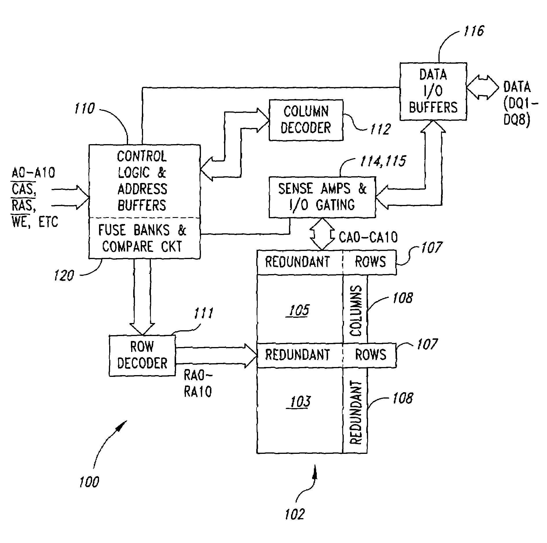
[0030]Referring to FIG. 1, a memory device 100 includes one or more memory arrays 102 each having primary memory sub-arrays such as two sub-arrays 103 and 105. Each of the primary memory sub-arrays 103 and 105 has redundant rows 107 and redundant columns 108 of memory cells. As described above, the redundant rows and columns 107 and 108 are selectively enabled to replace defective rows or columns of memory cells, respectively, in the primary memory sub-arrays 103 and 105.

[0031]Control logic and address buffer circuitry 110 receives externally applied signals such as an 11-bit addresses word on address lines or pins A0–A10. The control logic and address buffer circuitry 110 also receives externally generated control signals such as column address strobe CAS, row address strobe RAS, write enable WE, and so forth, as is known by those skilled in the relevant art. When the control logic and address buffer circuitry 110 receives the addresses on address lines A0–A10, it buffers and latch...


PUM


Abstract

The present invention reduces the area on a die required for rows and columns of redundant memory cells by sharing compare circuitry with banks of redundant memory cells based on division of the primary memory array into two or more “planes.” Pass gates or multiplexers coupled between at least two banks of fuses and one compare circuit selectively couple the appropriate fuse bank to the compare circuit. Preferably, a bit in the address (e.g., address bit RA9 in a row address word having address bits A0-RA9) is received by and controls the multiplexer to select between the two banks of fuses. Additionally, the planes span blocks of memory in the memory array, where each block is divided by shared sense amplifiers. As a result, while eight lines are coupled to 16 rows or columns, only eight rows or columns will be active at any one time because isolation gates will enable only eight of the 16 rows or columns within two planes of memory. As a result, the present invention saves on the number of lines required to intercouple the compare circuits to the redundant rows/columns.

Description

CROSS-REFERENCE TO RELATED APPLICATIONS[0001]This application is a continuation of U.S. patent application Ser. No. 09 / 747,352, filed Dec. 19, 2000; issued May 6, 2003 as U.S. Pat. No. 6,560,728, which is a continuation of U.S. patent application Ser. No. 09 / 415,472, filed Oct. 8, 1999, issued Dec. 19, 2000 as U.S. Pat. No. 6,163,860, which is a continuation of U.S. patent application Ser. No. 08 / 911,669, filed Aug. 14, 1997, issued Jan. 25, 2000 as U.S. Pat. No. 6,018,811, which is a divisional of U.S. patent application Ser. No. 08 / 637,875, filed Apr. 25, 1996, issued Jan. 6, 1998 as U.S. Pat. No. 5,706,292.TECHNICAL FIELD[0002]The present invention relates to an apparatus and method for testing semiconductor electrical devices, particularly memory devices.BACKGROUND OF THE INVENTION[0003]Testing is performed on semiconductor devices to locate defects and failures in such devices, typically occurring during the manufacture of the semiconductor devices. As circuit density on semico...

Claims


Application Information

Patent Timeline
IPC IPC(8): G11C29/00G06F12/16G06F11/20G06F12/00G11C5/00G11C7/10G11C11/401G11C29/04H01L21/82
CPCG11C7/1006G11C29/81G11C29/70G06F11/20
Inventor MERRITT, TODD A.
Owner MICRON TECH INC
Why Eureka
Try Eureka