Apparatus and method for forming a battery in an integrated circuit

Inactive Publication Date: 2006-05-16
GLOBALFOUNDRIES US INC
View PDF19 Cites 30 Cited by
  • Summary
  • Abstract
  • Description
  • Claims
  • Application Information

AI Technical Summary

Benefits of technology

[0019]The present invention supplies nonstandard bias voltages and nonstandard reference voltages in accordance with special requirements of particular integrated circuits. The present invention also avoids using

Problems solved by technology

For particular integrated circuit applications requiring nonstandard bias and nonsta

Method used


Image

  • Apparatus and method for forming a battery in an integrated circuit
  • Apparatus and method for forming a battery in an integrated circuit
  • Apparatus and method for forming a battery in an integrated circuit

Examples


Embodiment Construction

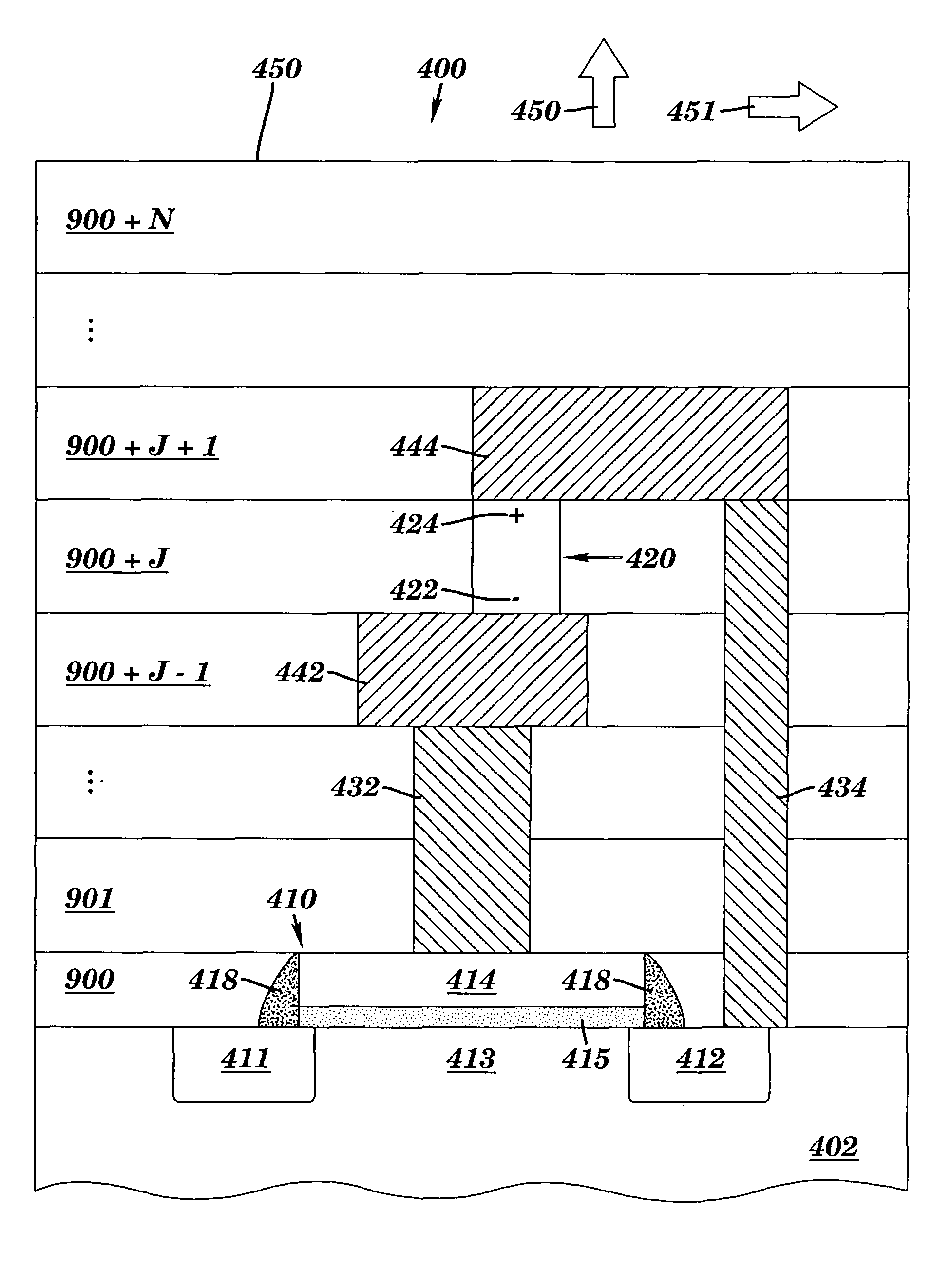
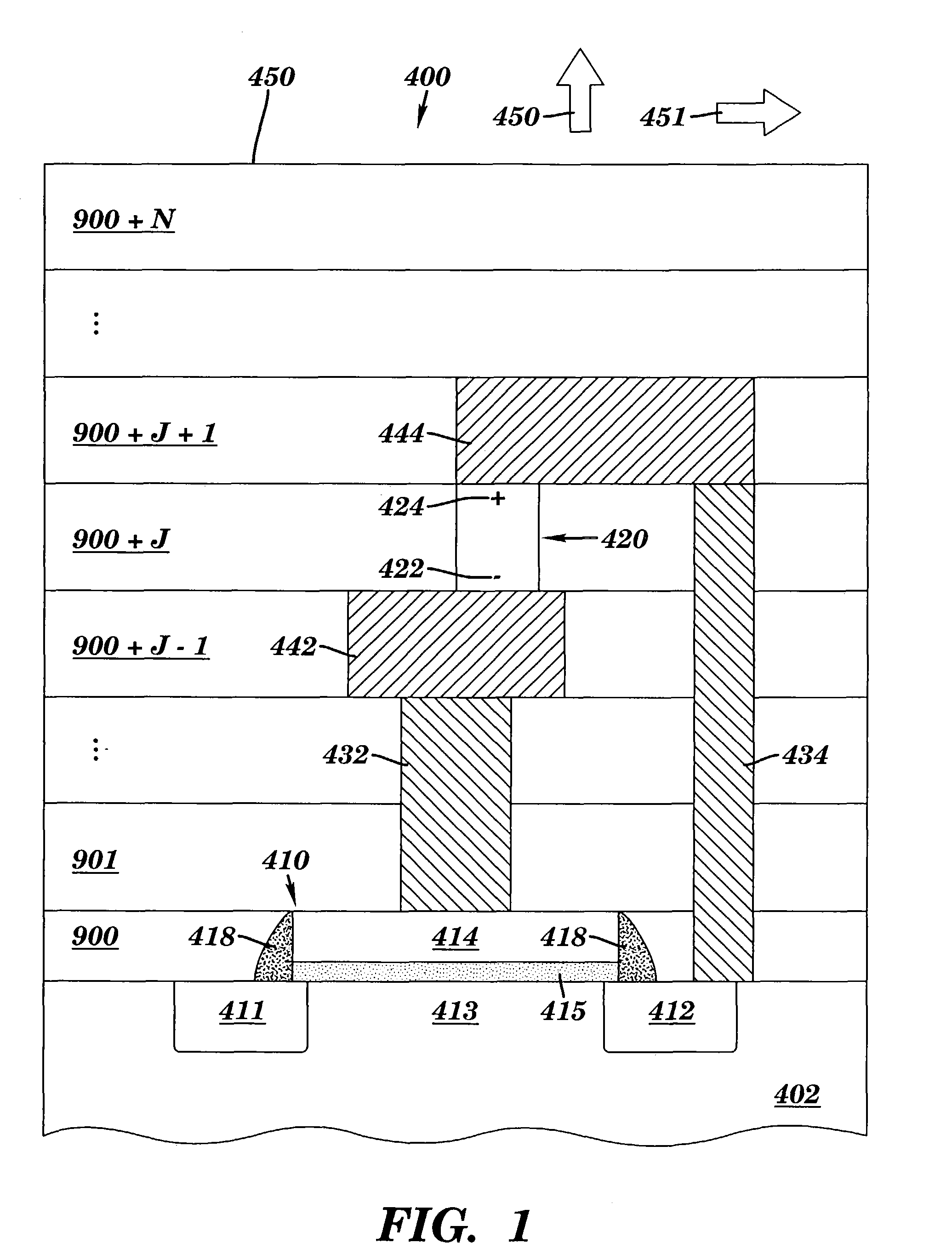
[0044]An integrated circuit may be fabricated by, inter alia, Front-End-Of-Line (FEOL) processing followed by Back-End-Of-Line (BEOL) integration. FEOL processing comprises forming a layer of electronic devices on a semiconductor wafer, which includes supporting process steps for defining the electronic devices (e.g., photolithography, annealing, ion implants, oxidation, etc.). The semiconductor wafer may include, inter alia, a bulk single-crystal silicon wafer with or without a buried oxide layer. The electronic devices include, inter alia, transistors, bipolar transistors, diodes, etc. BEOL integration conductively couples the electronic devices together to form completed electrical circuits, by forming a multilayered structure on and above the layer of electronic devices. Each layer of the multilayered structure may be thought of as a wiring level that includes conductive metallization (e.g., metal-plated vias, conductive wiring lines, etc.) embedded in insulative material (e.g.,...


PUM


Abstract

A method and structure that provides a battery within an integrated circuit for providing voltage to low-current electronic devices that exist within the integrated circuit. The method includes Front-End-Of-Line (FEOL) processing for generating a layer of electronic devices on a semiconductor wafer, followed by Back-End-Of-Line (BEOL) integration for wires connecting the electronic devices together to form completed electrical circuits of the integrated circuit. The BEOL integration includes forming a multilayered structure of wiring levels on the layer of electronic devices. Each wiring level includes conductive metallization (e.g., metal-plated vias, conductive wiring lines, etc.) embedded in insulative material. The battery is formed during BEOL integration within one or more wiring levels, and the conductive metallization conductively couples positive and negative terminals of the battery to the electronic devices. The battery may have several different topologies relative to the structural and geometrical relationships among the battery electrodes and electrolyte. Multiple batteries may be formed within one or more wiring levels, and may be conductively coupled to the electronic devices. The multiple batteries may be connected in series or in parallel.

Description

[0001]This application is a divisional of Ser. No. 09 / 761,123; filed on Jan. 16, 2001 now U.S. Pat. No. 6,650,000.BACKGROUND OF THE INVENTION[0002]1. Technical Field[0003]The present invention relates to a method and structure that provides a battery within an integrated circuit for providing voltage to low-current electronic devices that exist within the integrated circuit.[0004]2. Related Art[0005]An integrated circuit, which may include a semiconductor chip, comprises electronic devices on a bulk silicon wafer, and metallic wiring patterns which conductively couple the electronic devices, resulting in formation of electrical circuits. “Conductive” and like words means “electrically conductive” herein, unless otherwise stated. The electronic devices include field effect transistors, bipolar transistors, diodes, etc. The metallic wiring patterns include conductive wiring lines, metal-plated vias, etc. In integrated circuits, the metallic wiring patterns are multi-layered, wherein e...

Claims


Application Information

Patent Timeline
IPC IPC(8): H01L21/00H01L21/822H01L21/768H01L23/522H01L23/58H01L27/04H01M4/58H01M6/02H01M6/18H01M6/42H01M10/052H01M10/0562H01M10/058H01M10/36H01M10/42
CPCH01L23/522H01L23/58H01M4/5825H01M10/052H01M10/425H01M6/42H01M10/0562H01L2924/0002H01M10/058Y02E60/122H01L2924/00Y02E60/10Y02P70/50H01L21/3205
Inventor BALLANTINE, ARNE W.GROVES, ROBERT A.LUND, JENNIFER L.NAKOS, JAMES S.RICE, MICHAEL B.STAMPER, ANTHONY K.
Owner GLOBALFOUNDRIES US INC
Why Eureka
Try Eureka