Light emitting device, method of driving a light emitting device, element substrate, and electronic equipment

Inactive Publication Date: 2006-05-16
SEMICON ENERGY LAB CO LTD
View PDF51 Cites 119 Cited by
  • Summary
  • Abstract
  • Description
  • Claims
  • Application Information

AI Technical Summary

Benefits of technology

[0050]In a pixel having the first or second structure of the present invention described above, a current supplied to the pixel does not flow into its light emitting element when the current supplied to the pixel is converted into a voltage by the first means. Therefore the time required to stabilize the voltage converted from the supplied current is not influenced by a capacitor of the light emitting element. Compared to the pixel shown in FIG. 27B, a pixel of the present invention is quicker in stabilizing the voltage converted from the supplied current and therefore a current can be written in a shorter period of time and after image is prevented from being recognized in animation display.
[0051]A light emitting device of the present invention also has the advantage of conventiona

Problems solved by technology

However, electric characteristics of polysilicon TFTs are far behind the electric characteristics of MOS transistors that are formed on single crystal silicon substrates.
Furthermore, polysilicon TFTs are easily fluctuated in characteristics because of defects in grain boundaries.
However, the two pixels of FIGS. 26A and 26B also have problems.
Then the amount of current supplied to the light emitting element from the

Method used


Image

  • Light emitting device, method of driving a light emitting device, element substrate, and electronic equipment
  • Light emitting device, method of driving a light emitting device, element substrate, and electronic equipment
  • Light emitting device, method of driving a light emitting device, element substrate, and electronic equipment

Examples


embodiment mode 1

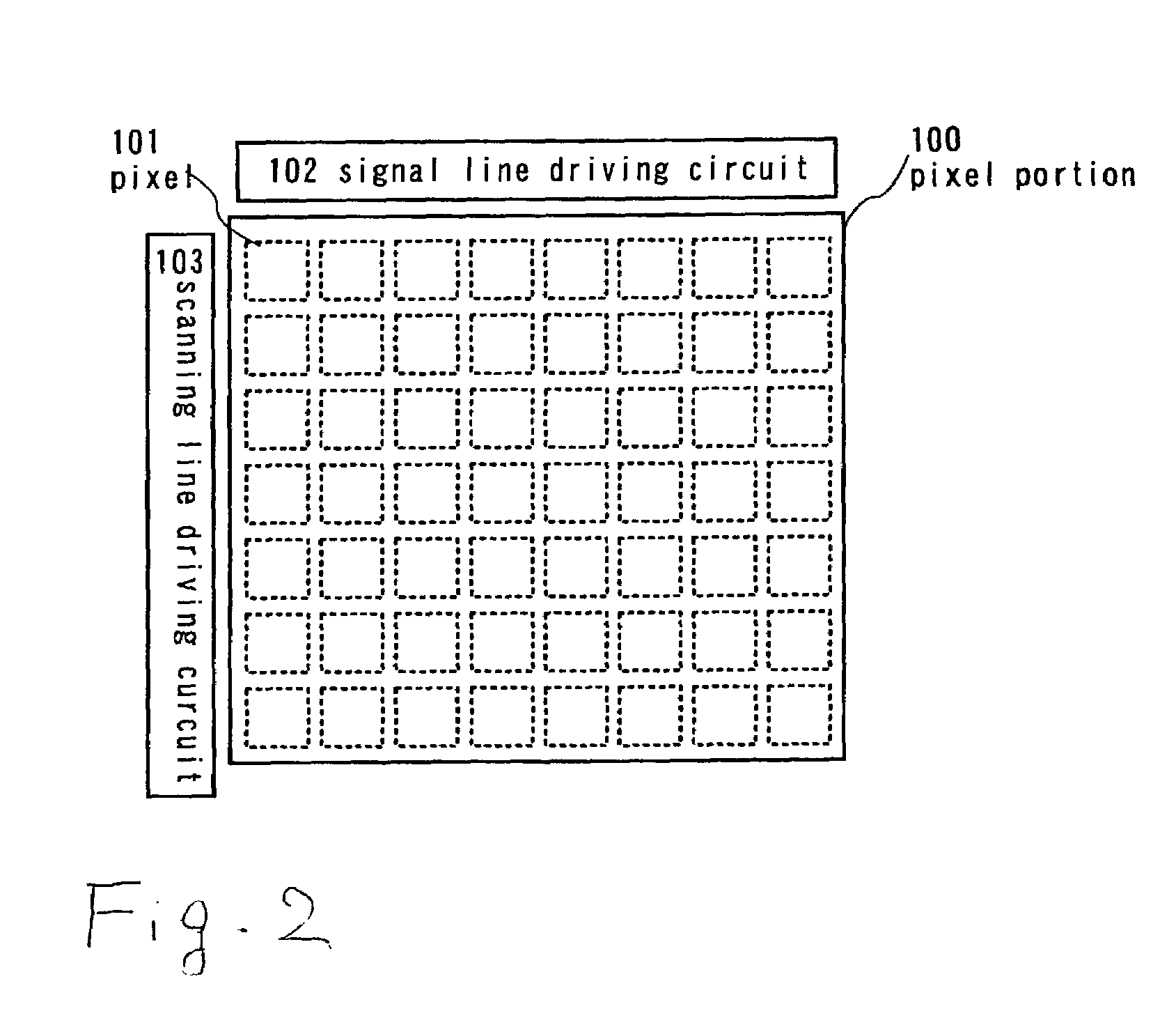
[0091]FIG. 2 is a block diagram showing the structure of a light emitting panel of the present invention. Denoted by 100 is a pixel portion in which a plurality of pixels form a matrix pattern. Each pixel is denoted by 101. 102 denotes a signal line driving circuit and 103 denotes a scanning line driving circuit.

[0092]In FIG. 2, the signal line driving circuit 102 and the scanning line driving circuit 103 are formed on the same substrate where the pixel portion 100 is formed. However, the present invention is not limited thereto. The signal line driving circuit 102 and the scanning line driving circuit 103 may be formed on a substrate different from the one on which the pixel portion 100 is formed, and may be connected to the pixel portion 100 through a connector such as an FPC. The device in FIG. 2 has one signal line driving circuit 102 and one scanning line driving circuit 103. However, the present invention is not limited thereto and the number of signal line driving circuit 102...

embodiment mode 2

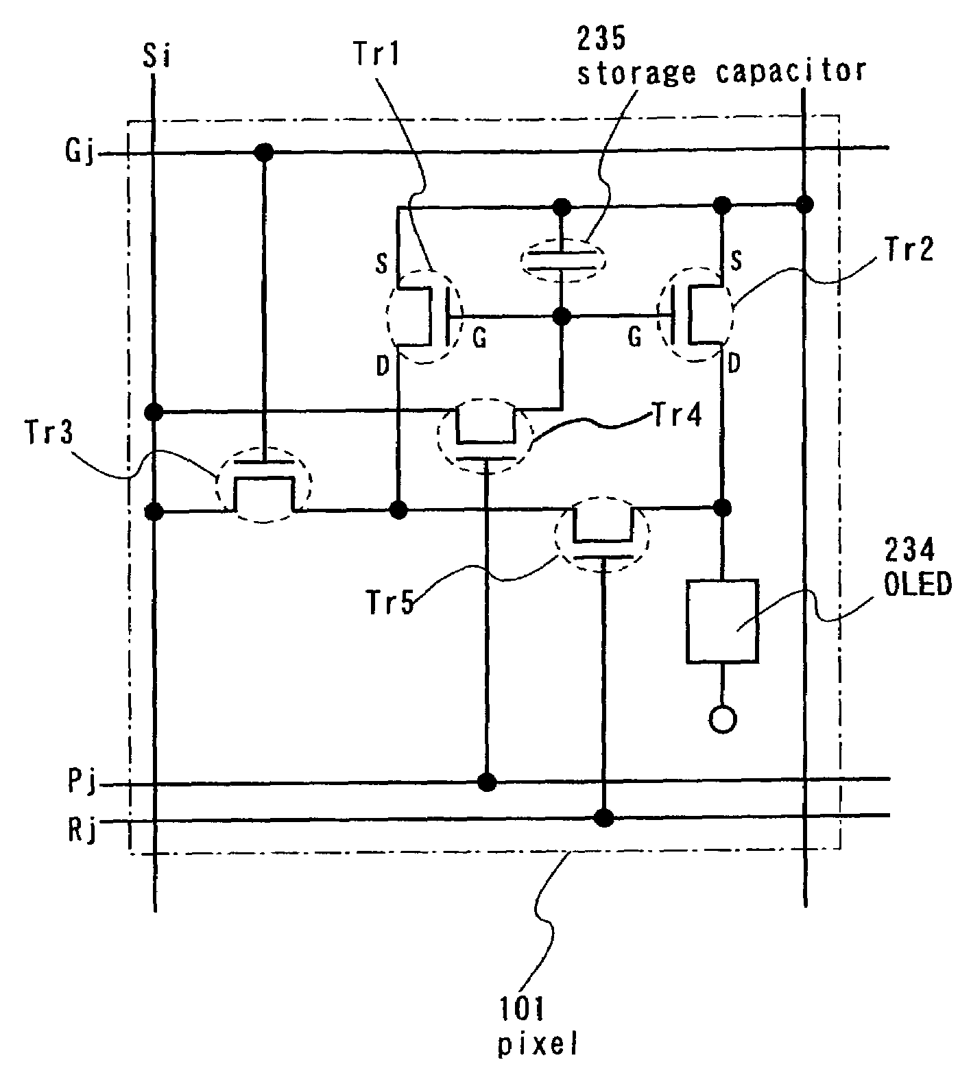
[0131]Shown in FIG. 3 is one structure of the pixel 101 of the light emitting device of FIG. 2. This embodiment mode gives a description on another structure of this pixel 101.

[0132]FIG. 6 shows a detailed structure of the pixel 101 in FIG. 2. The pixel 101 shown in FIG. 6 has a signal line Si (one of S1 to Sx), a first scanning line Gj (one of G1 to Gy), a second scanning line Pj (one of P1 to Py), a third scanning line Rj (one of R1 to Ry), and a power supply line Vi (one of V1 to Vx).

[0133]The pixel 101 also has a transistor Tr1, a transistor Tr2, a transistor Tr3, a transistor Tr4, a transistor Tr5, a transistor Tr6, a light emitting element 214, and a storage capacitor 215. The storage capacitor 215 is provided to hold the gate voltage of the transistors Tr1 and Tr2 more securely, but it is not always necessary.

[0134]A gate of the transistor Tr3 is connected to the first scanning line Gj. The transistor Tr3 has a source and a drain one of which is connected to the signal line S...

embodiment mode 3

[0169]Shown in FIGS. 3 and 6 are structures of the pixel 101 of the light emitting device of FIG. 2. This embodiment mode gives a description on still another structure of this pixel 101. This embodiment mode is obtained by changing the positions of Tr5 and Tr6 in FIG. 6. Alternatively, only one of Tr5 and Tr6 may change its position.

[0170]FIG. 8 shows a detailed structure of the pixel 101 shown in FIG. 2. The pixel 101 shown in FIG. 8 has a signal line Si (one of S1 to Sx), a first scanning line Gj (one of G1 to Gy), a second scanning line Pj (one of P1 to Py), a third scanning line Rj (one of R1 to Ry), and a power supply line Vi (one of V1 to Vx).

[0171]The pixel 101 also has a transistor Tr1, a transistor Tr2, a transistor Tr3, a transistor Tr4, a transistor Tr5, a transistor Tr6, a light emitting element 224, and a storage capacitor 225. The storage capacitor 225 is provided to hold the gate voltage of the transistors Tr1 and Tr2 more securely, but it is not always necessary.

[01...


PUM


Abstract

A display device capable of obtaining a constant luminance without being influenced by temperature change is provided as well as a method of driving the display device. A current mirror circuit composed of a first transistor and a second transistor is provided in each pixel. The first transistor and second transistor of the current mirror circuit are connected such that their drain currents are kept almost equal irrespective of the level of load resistance. By controlling the OLED drive current using the current mirror circuit, a change in OLED drive current due to fluctuation in characteristics between transistors is avoided and a constant luminance is obtained without being influenced by temperature change.

Description

BACKGROUND OF THE INVENTION[0001]1. Field of the Invention[0002]The present invention relates to a light emitting panel in which a light emitting element formed on a substrate is enclosed between the substrate and a cover member. Also, the present invention relates to a light emitting module in which an IC or the like is mounted on the light emitting panel. Note that, in this specification, the light emitting panel and the light emitting module are generically called light emitting devices. The present invention further relates to a method of driving the light emitting device and an electronic appliance using the light emitting device. Moreover, present invention relates to an element substrate corresponding to one mode before the light emitting element is completed in the step of manufacturing the light emitting device, wherein said element substrate includes means for providing electric current to the light emitting element in a plurality of pixels, respectively.[0003]2. Descripti...

Claims


Application Information

Patent Timeline
IPC IPC(8): G09G5/00H05B44/00G09G3/20G09G3/32H01L21/336H01L21/77H01L21/84H01L27/12H01L27/32H01L29/423H01L29/49H01L29/786H01L51/52
CPCG09G3/2022G09G3/3283H01L29/42384H01L29/4908H01L29/66757H01L29/78621G09G3/3208G09G3/3225G09G3/3241H01L2029/7863G09G2300/0814G09G2300/0842G09G2300/0861G09G2310/061G09G2320/0233H01L27/12H01L27/1214H01L27/3244H01L51/5237H10K59/12H10K50/841H10K50/846H10K50/844G09G3/20H10K50/84
Inventor KIMURA, HAJIME
Owner SEMICON ENERGY LAB CO LTD
Why Eureka
Try Eureka