Scintillation crystal detection arrays for radiation imaging devices

a technology of radiation imaging and scintillation crystals, applied in the field of high-resolution radiation imaging, can solve the problems of small fraction of scintillation light produced in the crystal to reach the photodetector, affecting the detection sensitivity of conventional discrete crystal designs, and worsening of light loss problems associated with standard photodetector readout at the end of the scintillating crystal

Active Publication Date: 2006-05-23
THE BOARD OF TRUSTEES OF THE LELAND STANFORD JUNIOR UNIV
View PDF7 Cites 21 Cited by
  • Summary
  • Abstract
  • Description
  • Claims
  • Application Information

AI Technical Summary

Benefits of technology

[0013]A radiation imaging device includes scintillation crystal sheets arranged in parallel to each other. Semiconductor photodetector positional detectors read light from large faces of the scintillation crystal sheets to detect interactions in the scintillation crystal sheets and independently provide positional information concerning the interactions relative to at least one axis. The structures of the photodetectors and crystal sheets provide for very small spaces between the sheets.

Problems solved by technology

Detection sensitivity in the conventional discrete-crystal designs is hampered by coupling of the scintillation crystals to the PMTs.
However, for very fine crystals in high resolution PET systems only a small fraction of the scintillation light produced in the crystal reaches the photodetector.
This light loss problem associated with standard photodetector readout at the end of the scintillating crystal worsens as the crystal is made narrower and longer or has untreated surfaces.
This light loss problem together with the low quantum efficiency of the PMT photocathode for detecting the scintillation light produced limits the count efficiency and signal-to-noise ratio of both the crystal decoding scheme used to position and time an annihilation photon event, and the energy (spectral) resolution required to reduce gamma-ray scatter and random coincidence background rates.
An additional related problem associated with the conventional end readout is that the light collection efficiency depends on the location within the crystal where light was created and thus, where the radiation interacted.
This factor further degrades the energy resolution.
Also, there is roughly a 10–15% light loss at the interface between the crystal and PMT due to index of refraction mismatches, further degrading the signal to noise ratio.
In a particular commercial high resolution design, additional fiber optics are included between the crystals and the PMT, which further degrades the available light signal.
Extracting a high fraction of the available scintillation light from the ends of long and narrow crystals proves to be very difficult due to a poor aspect ratio for light collection.
The result is lower signal to noise ratios (S / N), relatively small pulse heights (reduced sensitivity), and inadequate energy resolution (reduced Compton scatter and random photon rejection capabilities).
This low light extraction also contributes to non-optimized coincidence time and spatial resolution.
To facilitate light collection, the crystal sides must be highly polished, which significantly increases complexity and costs.
Detection sensitivity, though, is another limiting factor.
To maintain high detection sensitivity and good image quality, the challenges are to develop a finely pixellated scintillation crystal array with both high detection efficiency and high light collection.
A difficulty with designs having small scintillation crystals for high resolution is that manufacturing is a significant challenge.
It is costly and complex to handle many minute crystal elements and align them with corresponding photodetector elements.
Slight misalignments might reduce light collection efficiency.
Thus, crystal sheet detectors that have been used in PET suffer from low efficiency for stopping the high energy photons.

Method used


Image

  • Scintillation crystal detection arrays for radiation imaging devices
  • Scintillation crystal detection arrays for radiation imaging devices
  • Scintillation crystal detection arrays for radiation imaging devices

Examples


Embodiment Construction

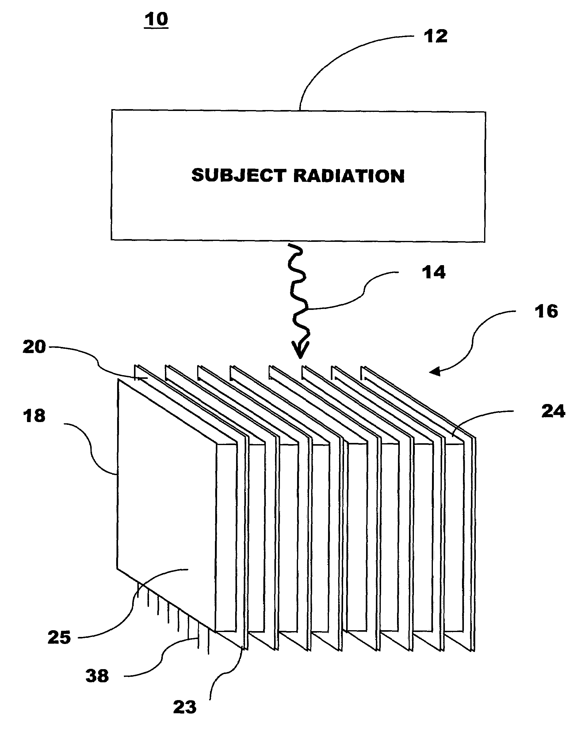
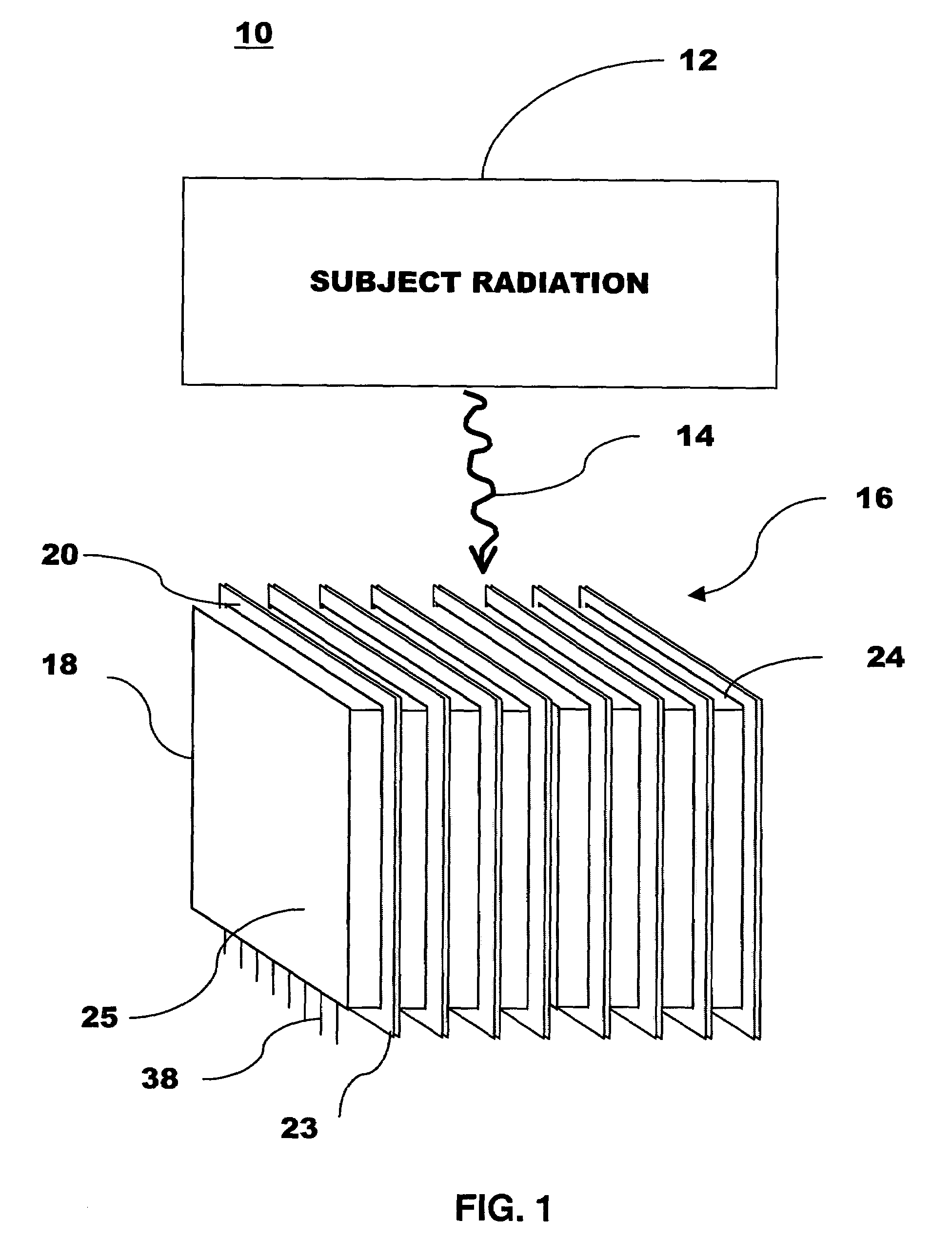
[0025]The invention relates to scintillation crystal arrays and imaging devices using scintillation crystal arrays. A scintillation crystal array of the invention increases light collection, can obtain near complete light collection, and improves detection, count efficiency, spatial resolution, and analysis of penetrating radioactive emissions. A preferred application of the invention is Positron Emission Tomography (PET).

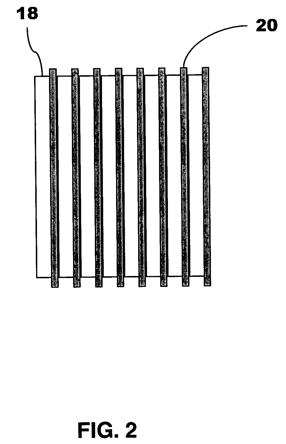
[0026]A preferred embodiment of the invention includes an array of scintillation crystal sheets arranged in a device such that radiation is incident upon small end faces of the sheets. Semiconductor photodiodes read light from large faces of crystal sheets. The semiconductor photodiodes may be pixellated, meaning that the semiconductor photodiodes provide both detection of photons generated in the scintillation crystals and positional information about a detection, or may be one large pixel with positioning capability within that pixel In another preferred embodime...


PUM


Abstract

A radiation imaging device includes scintillation crystal sheets arranged in parallel to each other. Semiconductor photodetector positional detectors read light from large faces of the scintillation crystal sheets to detect interactions in the scintillation crystal sheets and independently provide positional information concerning the interactions relative to at least one axis. The structures of the photodetectors and crystal sheets provide for very small spaces between the sheets.

Description

REFERENCE TO RELATED APPLICATION AND PRIORITY CLAIM[0001]This application is related to pending provisional application Ser. No. 60 / 411,613 filed on Sep. 18, 2002, and claims priority from that provisional application under 35 U.S.C. §119.FIELD OF THE INVENTION[0002]The field of the invention is high resolution radiation imaging. An exemplary application of the invention is a Positron Emission Tomography (PET) device.BACKGROUND OF THE INVENTION[0003]Scintillation crystals are commonly used in non-invasive medical diagnostic techniques that utilize radiation emitting materials. These crystals are noted for their ability to emit pulses of visible light when ionizing radiation, such as gamma radiation, passes therethrough and interacts with atomic nuclei in the crystal. The pulses of emitted light (photons) are then detected by a photodetector device such as a photomultiplier tube (PMT) or a semiconductor photodiode (SPD). The effectiveness of the detector in diagnostic procedures depe...

Claims


Application Information

Patent Timeline
Patent Type & Authority Patents(United States)
IPC IPC(8): G01T1/166G01T1/20
CPCG01T1/2018G01T1/20187G01T1/20181G01T1/20182
Inventor LEVIN, CRAIG S.
Owner THE BOARD OF TRUSTEES OF THE LELAND STANFORD JUNIOR UNIV
Why Eureka
Try Eureka