Photoelectric detection device and method for its production

Inactive Publication Date: 2006-05-23
COMMISSARIAT A LENERGIE ATOMIQUE ET AUX ENERGIES ALTERNATIVES
View PDF6 Cites 3 Cited by
  • Summary
  • Abstract
  • Description
  • Claims
  • Application Information

AI Technical Summary

Benefits of technology

[0021]It is an object of the present invention to obviate these various drawbacks. It firstly relates to structuring of the surface

Problems solved by technology

One of the problems often encountered with this type of structure involves the inter-pixel leakage currents at the lower electrodes, in particular due to the appearance of a potential difference between two neighbouring lower electrodes.
Matrixing the sensitive layers, however, presents the drawback of demanding regrowth on each level which is intended to be matrixed.
It is found that the problems inherent in contamination of the surface and of repeated contact have the effect of increasing the dark current of the detectors obtained in this way, and therefore their sensitivity in respect of weak illumination.
Another difficulty to be surm

Method used


Image

  • Photoelectric detection device and method for its production
  • Photoelectric detection device and method for its production

Examples


Embodiment Construction

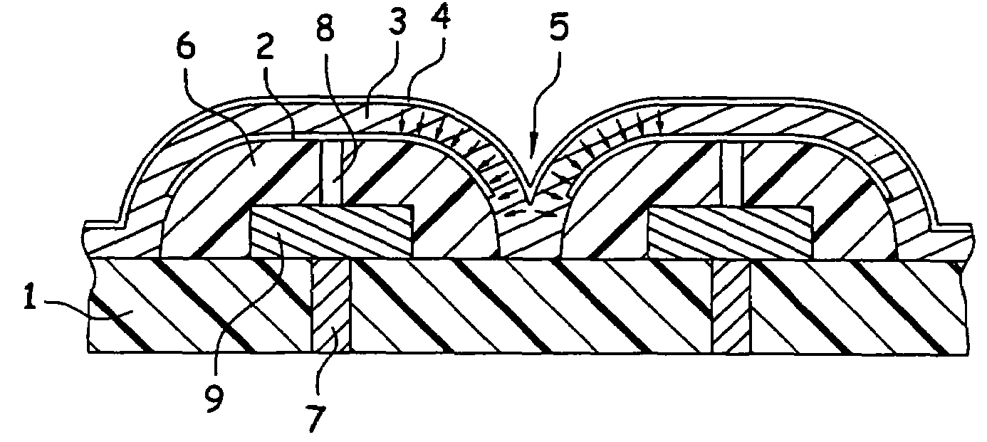
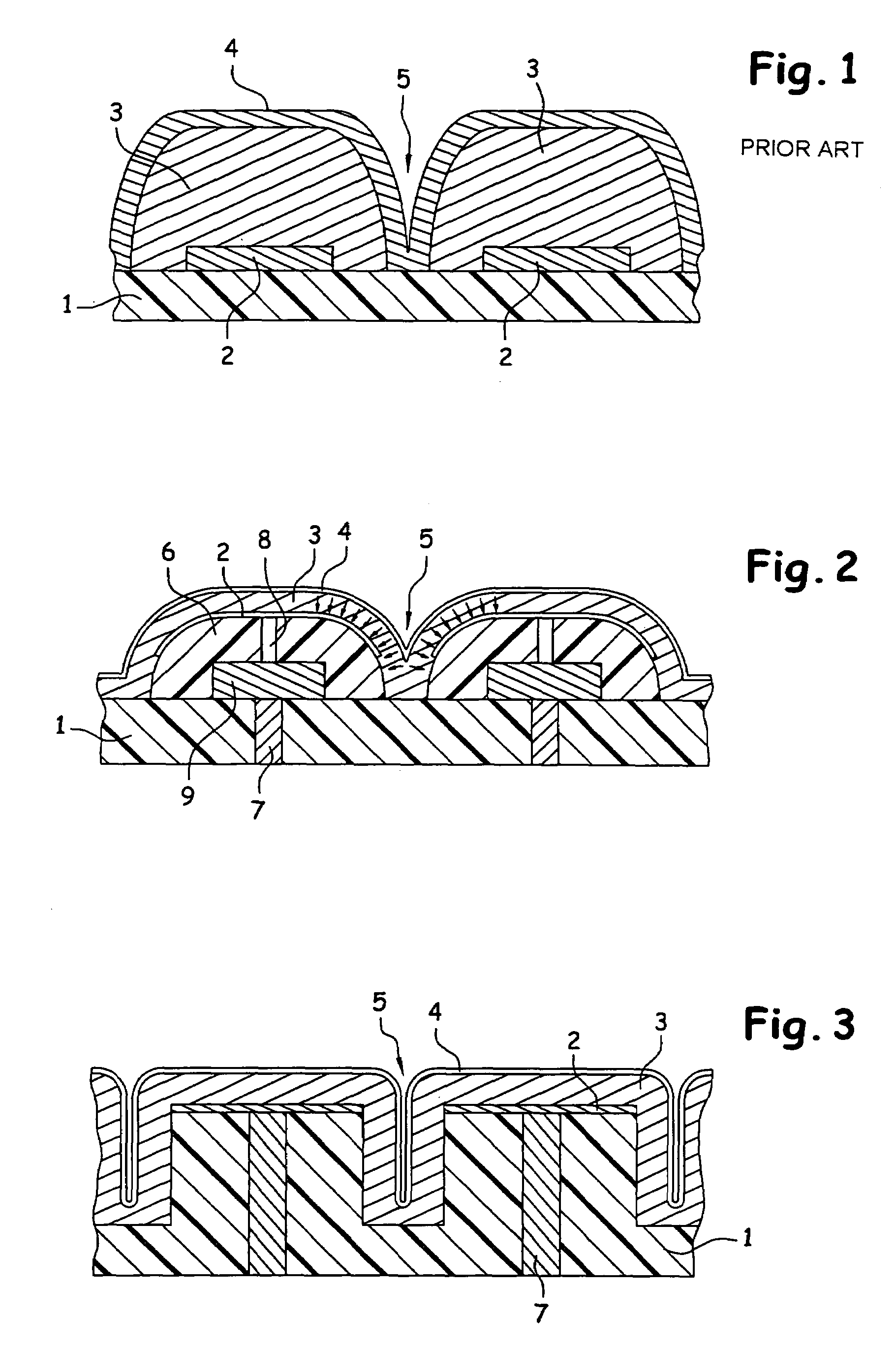
[0055]The photoelectric detector according to the invention has therefore been represented in relation to FIG. 2. In order to simplify the schematic representation, the sense circuit has not been represented in this figure. Furthermore, the various numerical references corresponding to elements or components which are identical to those of the prior art have been retained.

[0056]According to the invention, for each pixel, the photoelectric detector firstly includes a metallization layer (9) with a relatively large thickness, typically 1 μm, which is connected to the sense circuit by means of a conductor or “plug” (7).

[0057]This metallization layer (9) is then enclosed in an insulator deposit (6), such as a silicon oxide, a silicon nitride, a silicon oxynitride or any combination thereof. This insulator deposit (6) therefore comes into contact with the silicon of the insulating support (1), and constitutes a convexly shaped zone as can be seen in FIG. 2. This deposit (6) may be produc...


PUM


Abstract

This photoelectric detection device comprises a matrix of elementary detectors on an insulating substrate. Each of the elementary detectors has a stack consisting of a lower electrode, a layer of a photosensitive material and a phototransparent upper electrode. The upper electrode is common to all the elementary detectors. Each of the lower electrodes is connected independently of one another to a sense circuit. The lower electrodes are each positioned on an individualized insulating zone, which is raised with respect to the insulating substrate. Furthermore, the upper electrode is not flat and is inserted between two adjacent zones until it reaches a level below that of the lower electrodes.

Description

[0001]This application claims the benefit of French Application 02.15023, filed Nov. 29,2002, the entirety of which is incorporated herein by reference.FIELD OF THE INVENTION[0002]The field of the invention is that of optical detectors conventionally comprising a detection layer associated with a sense circuit, in particular one produced according to the so-called “above IC” structure, i.e. above an integrated circuit, in the field of microelectronics.BACKGROUND OF THE INVENTION[0003]Optical detectors are conventionally intended to detect a light intensity and to convert it into an electrical signal, the amplitude of which is proportional to the detected light intensity. These electrical signals are generally processed, particularly in the sense circuit, in order to reproduce an image of the detected scene.[0004]With a view to miniaturizing these detection devices, attempts have been made to integrate the actual detection with the signal processing circuit associated with it.[0005]T...

Claims


Application Information

Patent Timeline
IPC IPC(8): H01L31/117H01L27/144H01L27/14H01L27/146H01L31/0224H01L31/0328H01L31/0352H01L31/10
CPCH01L27/1446H01L31/022408H01L31/035281H01L31/03529Y02E10/50
Inventor MOUSSY, NORBERTGUEDJ, CYRIL
Owner COMMISSARIAT A LENERGIE ATOMIQUE ET AUX ENERGIES ALTERNATIVES
Why Eureka
Try Eureka