Semiconductor device with a voltage detecting device to prevent shoot-through phenomenon in first and second complementary switching devices

a technology of voltage detection and semiconductor devices, applied in the direction of logic circuit coupling/interface arrangements, pulse techniques, animal watering devices, etc., can solve the problems of large current flowing into the igbt, short circuit of high side igbt, and failure of high side gate drivers to continue outputting, so as to prevent damage to the semiconductor device and high voltage

Active Publication Date: 2006-05-23
ARIGNA TECH LTD
View PDF8 Cites 30 Cited by
  • Summary
  • Abstract
  • Description
  • Claims
  • Application Information

AI Technical Summary

Benefits of technology

[0009]An object of the present invention is to provide a high voltage integrated circuit for preventing damage to a semiconductor device used for performing bridge rectification of a power line.
[0011]The voltage detecting device provided in the low potential part detects the potential at an output line of at least one of the first and second level shift parts, that is, the high main power potential. Therefore, in the case where ground-fault occurs at the node between the first and second switching devices, the second pulse signal is generated at that timing to bring the high side switching device into a non-conducting state. Thus, phase fault protection for the high side switching device can be realized at low costs.
[0013]The voltage detecting device provided in the high potential part detects the potential at an output line of the reverse level-shift part, that is, the high main power potential. Therefore, in the case where ground-fault occurs at the node between the first and second switching devices, the control part controls the high side switching device for bringing it into a non-conducting state at that timing, so that the high side switching device is immediately brought into a non-conducting state. Thus, phase fault protection for the high side switching device can effectively be achieved.
[0015]The voltage detecting device detects the potential at an output line extending out of the high potential part and outputting the high main power potential, that is, the high main potential. Therefore, in the case where ground-fault occurs at the node between the first and second switching devices, the second pulse signal is generated at that timing to bring the high side switching device into a non-conducting state. Thus, phase fault protection for the high side switching device can be achieved. Further, detection of the potential at the output line extending out of the high potential part increases flexibility in arrangement of the voltage detecting device.
[0017]The voltage detecting device detecting the potential at the node between the first and second switching devices for controlling conduction / non-conduction of the high side switching device is provided in the high potential part. Therefore, in the case where ground-fault occurs at the node between the first and second switching devices, the control part is caused to control the high side switching device for bringing it into a non-conducting state at that timing, so that the high side switching device is immediately brought into a non-conducting state. Thus, phase fault protection for the high side switching device can effectively be achieved.

Problems solved by technology

In this HVIC, when a high side IGBT and a low side IGBT are brought into an on state at the same time (which is called a “shoot-through” phenomenon), short-circuit occurs between arms (power lines) to cause a large current to flow into the IGBTs, which are therefore damaged.
However, since the gate driver outputs are not monitored in practice, the high side IGBT is short-circuited in the case where a potential at a node between the high side IGBT and low side IGBT (hereinafter referred to as “potential VS”) is short-circuited to a ground potential (GND) (i.e., ground-fault occurs) due to failure in loads or the like while the high side gate driver continues outputting (i.e., while the high side IGBT is in an ON state).
Therefore, the high side IGBT needs to be turned off immediately, however, the HVIC is incapable of determining that the potential VS has become GND, and therefore causes the high side gate driver to continue outputting.
Thus, it is impossible to monitor the potential VS within the HVIC.
With this method, however, a certain period of time is required until a control signal is applied to the high side IGBT, during which short-circuit continues.
Therefore, the high side IGBT needs to have resistance to a short-circuit state for a certain period of time, which is a contributing factor responsible for increase in manufacturing costs.

Method used


Image

  • Semiconductor device with a voltage detecting device to prevent shoot-through phenomenon in first and second complementary switching devices
  • Semiconductor device with a voltage detecting device to prevent shoot-through phenomenon in first and second complementary switching devices
  • Semiconductor device with a voltage detecting device to prevent shoot-through phenomenon in first and second complementary switching devices

Examples


first preferred embodiment

1. Circuit Configuration

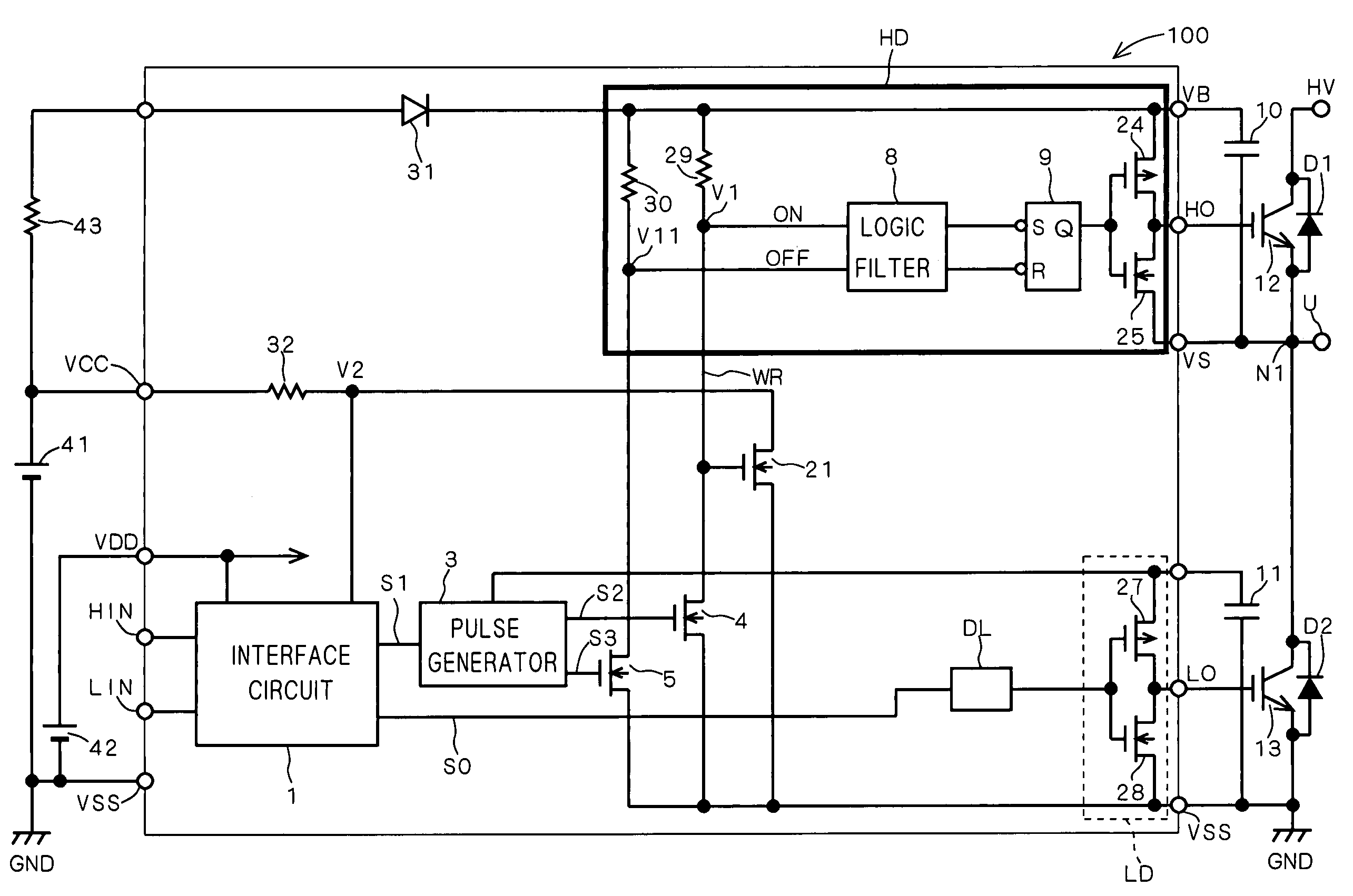
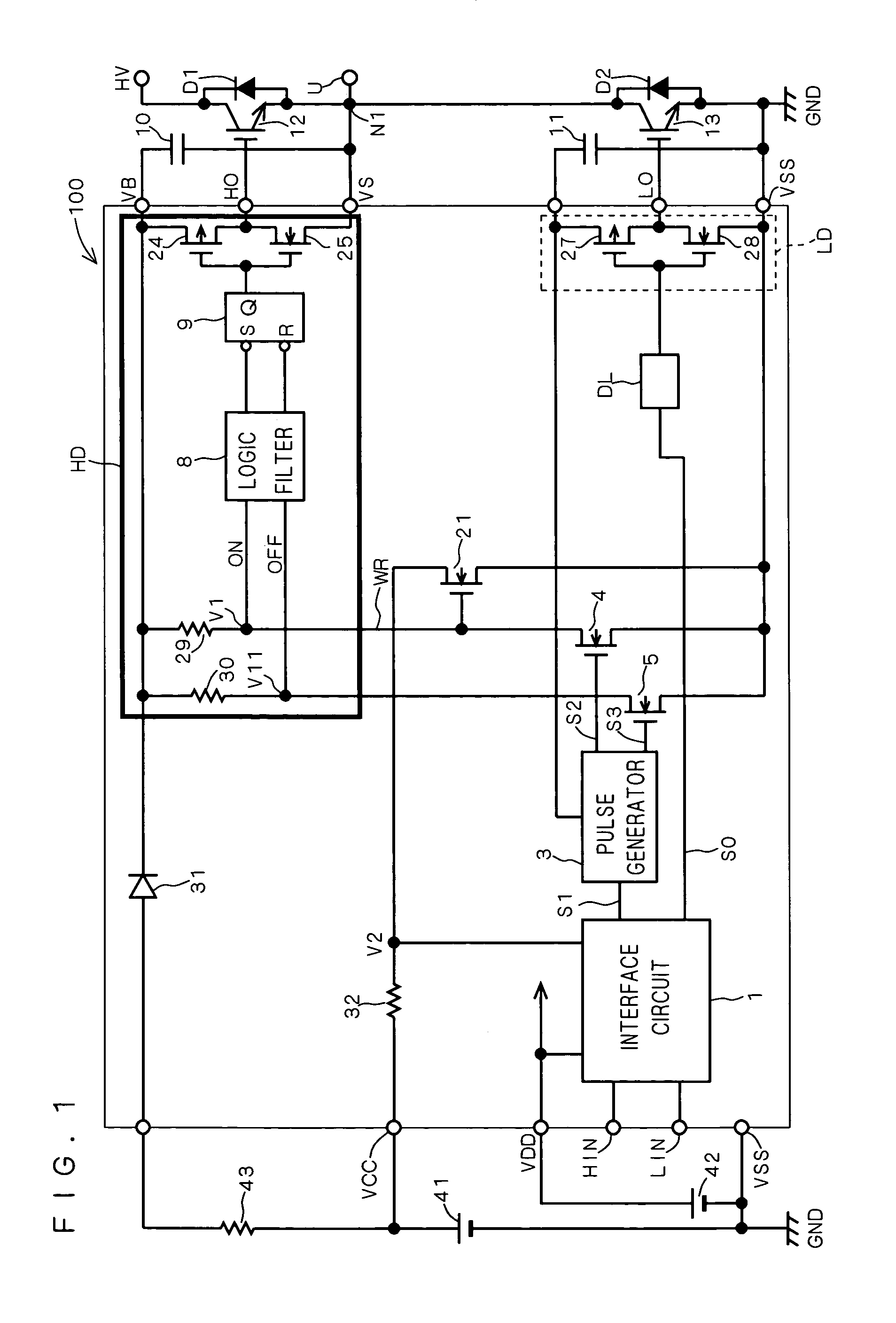
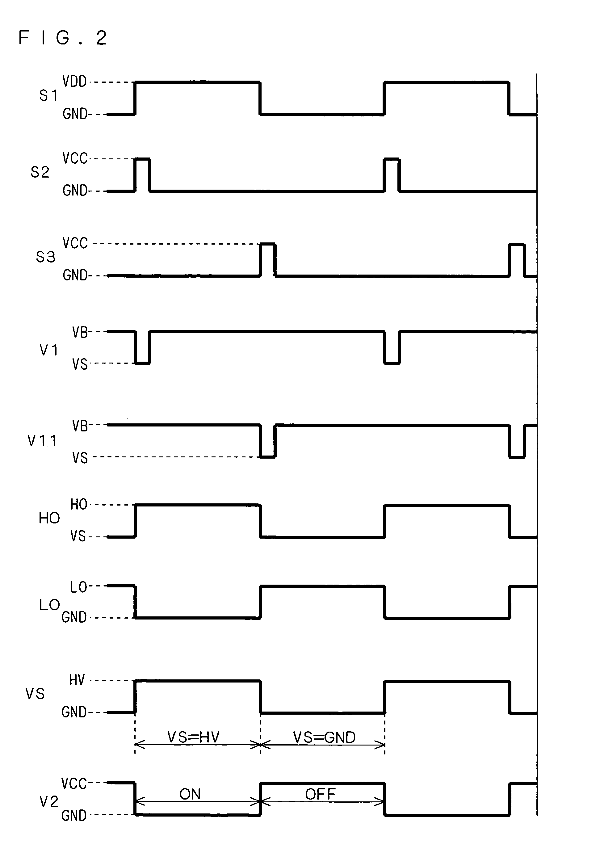
[0049]FIG. 1 illustrates the configuration of a high voltage integrated circuit (HVIC) 100 according to a first preferred embodiment of the present invention.

[0050]In FIG. 1, power devices 12 and 13 such as IGBTs (Integrated Gate Bipolar Transistors) are totem-pole-connected between a high side (HV) power line and a low (ground potential GND) side power line, to form a half-bridge power device. Free wheel diodes D1 and D2 are connected inversely in parallel to the power devices 12 and 13, respectively. Then, a load (an inductive load such as a motor) is connected to a node N1 between the power devices 12 and 13.

[0051]In FIG. 1, the power device 12 switches between a potential at the node N1 used as a reference potential and the potential (HV) at a high side power line, and is called a high side power device.

[0052]The power device 13 switches between the ground potential used as a reference potential and the potential at the node N1, and is called a low side p...

first modification

4. First Modification

[0119]Although the use of an NMOS transistor as a voltage detector has been described above by way of example, a PMOS transistor may be used instead. In this case, connecting the resistor 32 shown in FIG. 1 to the GND terminal, the drain of the PMOS transistor to the resistor 32, and the source to the VCC terminal, and performing a NAND operation of the drain potential V2 and HIN signal, the control signal S1 can be made an OFF signal at the timing when ground-fault occurs at the node N1.

[0120]Further, the use of an enhancement type MOS transistor as a voltage detector has been described by way of example, a depression type MOS transistor may be used instead.

[0121]When the potential VS becomes negative, an enhancement MOS transistor cannot detect it, however, a depression type MOS transistor, for example, is brought into an off state when the potential VS becomes negative, and thus can detect a negative potential VS.

second modification

5. Second Modification

[0122]Although the NMOS transistor 21 performing on / off control based on the drain potential at the HNMOS transistor 4 as shown in FIG. 1 has been described above, an NMOS transistor 22 performing on / off control based on the drain potential at the HNMOS transistor 5 may additionally be incorporated as in an HVIC 100A shown in FIG. 8.

[0123]In this case, the logic circuit voltage VCC is applied to the drain electrode of the NMOS transistor 22 through a resistor 33, and the ground potential is applied to the source electrode of the NMOS transistor 22. The potential VS is monitored indirectly also by monitoring a drain potential V22 at the NMOS transistor 22 by the interface circuit 1. Components shown in FIG. 8 similar to those in the HVIC 100 in FIG. 1 are indicated by the same reference numerals, repeated explanation of which is thus omitted here.

[0124]As described, providing a plurality of voltage detectors for monitoring the potential VS achieves redundancy, w...


PUM


Abstract

An HNMOS transistor (4) has its drain electrode connected to the gate electrode of an NMOS transistor (21), and a logic circuit voltage (VCC) is applied to the drain electrode of the NMOS transistor (21) through a resistor (32). A ground potential is applied to the source electrode of the NMOS transistor (21). A drain potential (V2) at the NMOS transistor (21) is monitored by an interface circuit (1), for indirectly monitoring a potential (VS). Thus provided is a high voltage integrated circuit for preventing damage to a semiconductor device used for performing bridge rectification of a power line.

Description

BACKGROUND OF THE INVENTION[0001]1. Field of the Invention[0002]The present invention relates to a semiconductor device, and more particularly, to a high voltage integrated circuit.[0003]2. Description of the Background Art[0004]A high voltage integrated circuit (HVIC) is a device indispensable for achieving great functionality and cost reduction in the field of mechatronics including motor control.[0005]For instance, an HVIC is employed as a gate driver in a power transistor such as an IGBT (Integrated Gate Bipolar Transistor) used for performing bridge rectification of a power line. In this HVIC, when a high side IGBT and a low side IGBT are brought into an on state at the same time (which is called a “shoot-through” phenomenon), short-circuit occurs between arms (power lines) to cause a large current to flow into the IGBTs, which are therefore damaged.[0006]To prevent this, the HVIC is controlled such that a high side gate driver output and a low side gate driver output are compl...

Claims


Application Information

Patent Timeline
Patent Type & Authority Patents(United States)
IPC IPC(8): H03K19/091H01L21/8234H01L21/8238H01L27/088H01L27/092H03K17/06H03K17/08H03K17/56H03K17/687H03K19/00
CPCH03K17/063H01L27/088A01K7/025
Inventor SHIMIZU, KAZUHIRO
Owner ARIGNA TECH LTD
Why Eureka
Try Eureka