Output driver circuit with reduced RF noise, reduced power consumption, and reduced load capacitance susceptibility

a technology of output driver and load capacitance, which is applied in the direction of oscillator, electronic switching, pulse technique, etc., can solve the problems of unsatisfactory radio frequency (rf) noise, harmonics generated by sharp edges of square waves, and increase the cost of the final product, so as to reduce power consumption, reduce load capacitance susceptibility, and reduce rf noise

Active Publication Date: 2006-05-23
SKYWORKS SOLUTIONS INC
View PDF7 Cites 14 Cited by
  • Summary
  • Abstract
  • Description
  • Claims
  • Application Information

AI Technical Summary

Benefits of technology

[0008]The present invention is directed to output driver circuit with reduced RF noise, reduced power consumption, and reduced load capacitance susceptibility. The present invention addresses and resolves the need in the art for an output driver circuit in an IC device, such as an ASIC, that generates reduced RF noise, consumes less power, and has reduced susceptibility to output load capacitance.

Problems solved by technology

However, the sharp edges of the square waves generate harmonics that create undesirable radio frequency (RF) noise.
The RF noise caused by harmonics generated by the sharp edges of the square waves can interfere with the RF-sensitive components, such as the RF receiver front end of a communication device.
However, both of the above isolation methods undesirably increase the cost of the final product.
However, filtering requires additional system board space and results in increased power consumption, while reducing the size of the output drivers leaves the output drivers more susceptible to load capacitance, which can prevent the output driver circuit from maintaining the required output data rate.
Additionally, reducing the size of the output drivers increases the crossover time in which both upper and lower output drive transistors are simultaneously on, which causes an undesirable increase in power consumption by increased “crowbar current.”

Method used


Image

  • Output driver circuit with reduced RF noise, reduced power consumption, and reduced load capacitance susceptibility
  • Output driver circuit with reduced RF noise, reduced power consumption, and reduced load capacitance susceptibility
  • Output driver circuit with reduced RF noise, reduced power consumption, and reduced load capacitance susceptibility

Examples


Embodiment Construction

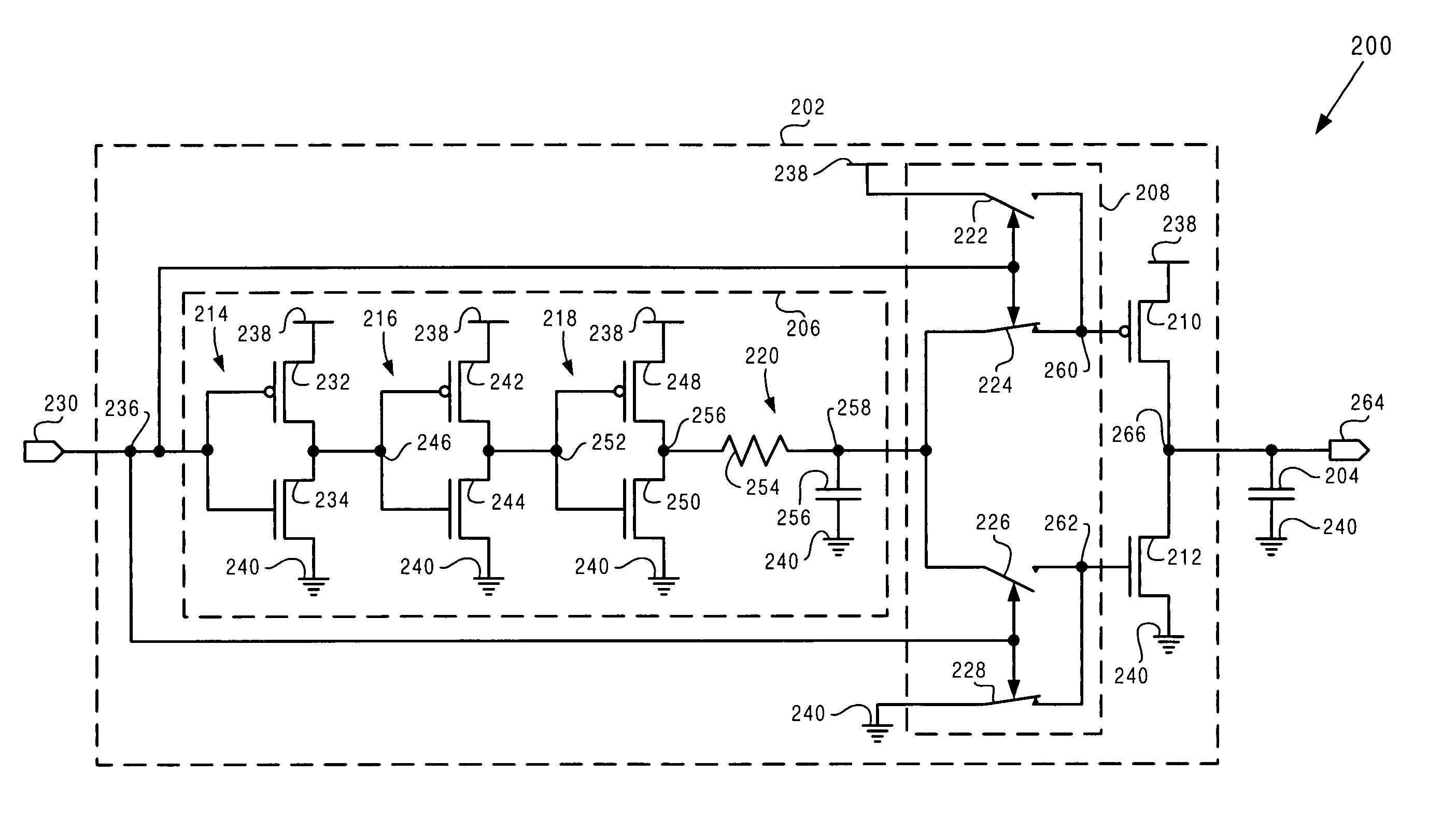
[0013]The present invention is directed to output driver circuit with reduced RF noise, reduced power consumption, and reduced load capacitance susceptibility. The following description contains specific information pertaining to the implementation of the present invention. One skilled in the art will recognize that the present invention may be implemented in a manner different from that specifically discussed in the present application. Moreover, some of the specific details of the invention are not discussed in order not to obscure the invention.

[0014]The drawings in the present application and their accompanying detailed description are directed to merely exemplary embodiments of the invention. To maintain brevity, other embodiments of the present invention are not specifically described in the present application and are not specifically illustrated by the present drawings.

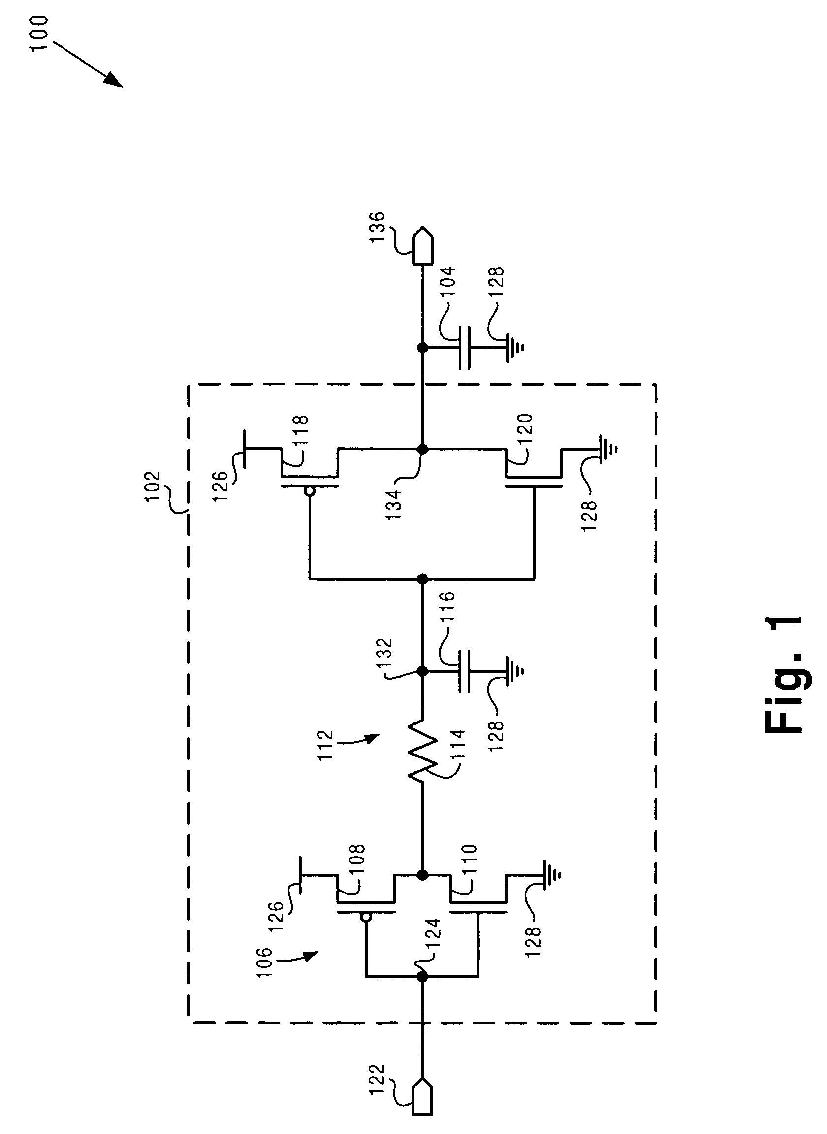
[0015]FIG. 1 shows a circuit diagram of an exemplary conventional output driver circuit coupled to a capaci...


PUM


Abstract

According to an exemplary embodiment, an output driver circuit includes a pre-conditioning circuit. The output driver circuit further includes a timing control circuit coupled to an output of the pre-conditioning circuit, where the timing control circuit has a first state and a second state. The output driver circuit further includes a first transistor having a first terminal coupled to the timing control circuit and a second transistor having a first terminal coupled to the timing control circuit. When the timing control circuit is in the first state the pre-conditioning circuit output is coupled to the first terminal of the first transistor and not coupled to the first terminal of the second transistor, and when the timing control circuit is in the second state the pre-conditioning circuit output is coupled to the first terminal of the second transistor and not coupled to the first terminal of the second transistor.

Description

BACKGROUND OF THE INVENTION[0001]1. Field of the Invention[0002]The present invention is generally in the field of semiconductor devices. More specifically, the invention is in the field of output drivers for semiconductor devices.[0003]2. Related Art[0004]Integrated circuit (IC) devices, such as application-specific ICs (ASICs), are typically utilized on system boards for communication devices, such as cellular handsets, as well as other types of electronic devices. These IC devices employ output driver circuits that have output drivers with fast edge rates to generate square wave logic outputs. However, the sharp edges of the square waves generate harmonics that create undesirable radio frequency (RF) noise. The RF noise caused by harmonics generated by the sharp edges of the square waves can interfere with the RF-sensitive components, such as the RF receiver front end of a communication device.[0005]One conventional approach to solving the RF noise problem discussed above include...

Claims


Application Information

Patent Timeline
Patent Type & Authority Patents(United States)
IPC IPC(8): H03B1/00H03K3/00
CPCH03K19/0013H03K17/163
Inventor BECHMAN, GARY S.YOUNG, JAMES P.
Owner SKYWORKS SOLUTIONS INC
Why Eureka
Try Eureka