Light emitting diodes with improved light extraction efficiency

a light-emitting diode and light-emitting technology, which is applied in the direction of semiconductor devices, electrical devices, instruments, etc., can solve the problems of compromising the reliability and performance of leds, adding additional losses due to total internal reflection at the epoxy/air interface, and reducing the light-emitting efficiency of light-emitting devices, so as to achieve the effect of improving the light-emitting efficiency of the light-emitting device and reducing loss

Inactive Publication Date: 2006-05-30
LUMILEDS
View PDF63 Cites 161 Cited by
  • Summary
  • Abstract
  • Description
  • Claims
  • Application Information

AI Technical Summary

Benefits of technology

[0015]Bonding a high refractive index lens to a light emitting device improves the light extraction efficiency of the light emitting device by reducing loss due to total internal reflection. Advantageously, this improvement can be achieved without the use of an encapsulant.

Problems solved by technology

Additional losses due to total internal reflection can occur at the epoxy / air interface.
However, this technique is tedious and wasteful of material.
In addition, defects introduced during the grinding process may compromise the reliability and performance of the LEDs.
However, shaping the surface of a low refractive index encapsulant such as epoxy does not reduce losses due to total internal reflection at the semiconductor / low index encapsulant interface.
Moreover, epoxy encapsulants typically have coefficients of thermal expansion that poorly match those of the semiconductor materials in the LED.
Consequently, the epoxy encapsulant subjects the LED to mechanical stress upon heating or cooling and may damage the LED.
Unfortunately, optical absorption in high index glasses and mechanical stress typically degrade the performance of an LED encapsulated in such glass.

Method used


Image

  • Light emitting diodes with improved light extraction efficiency
  • Light emitting diodes with improved light extraction efficiency
  • Light emitting diodes with improved light extraction efficiency

Examples


Embodiment Construction

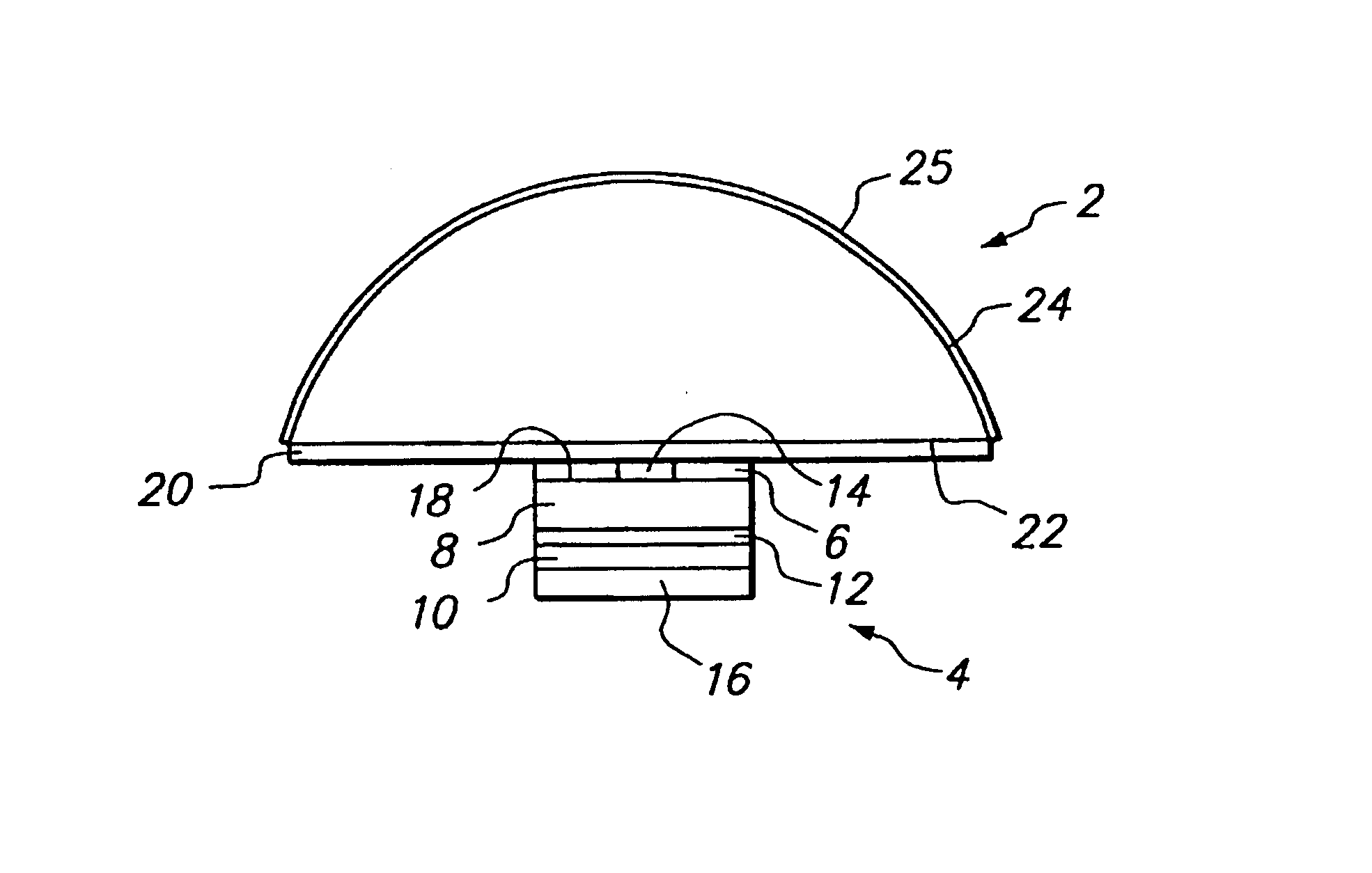
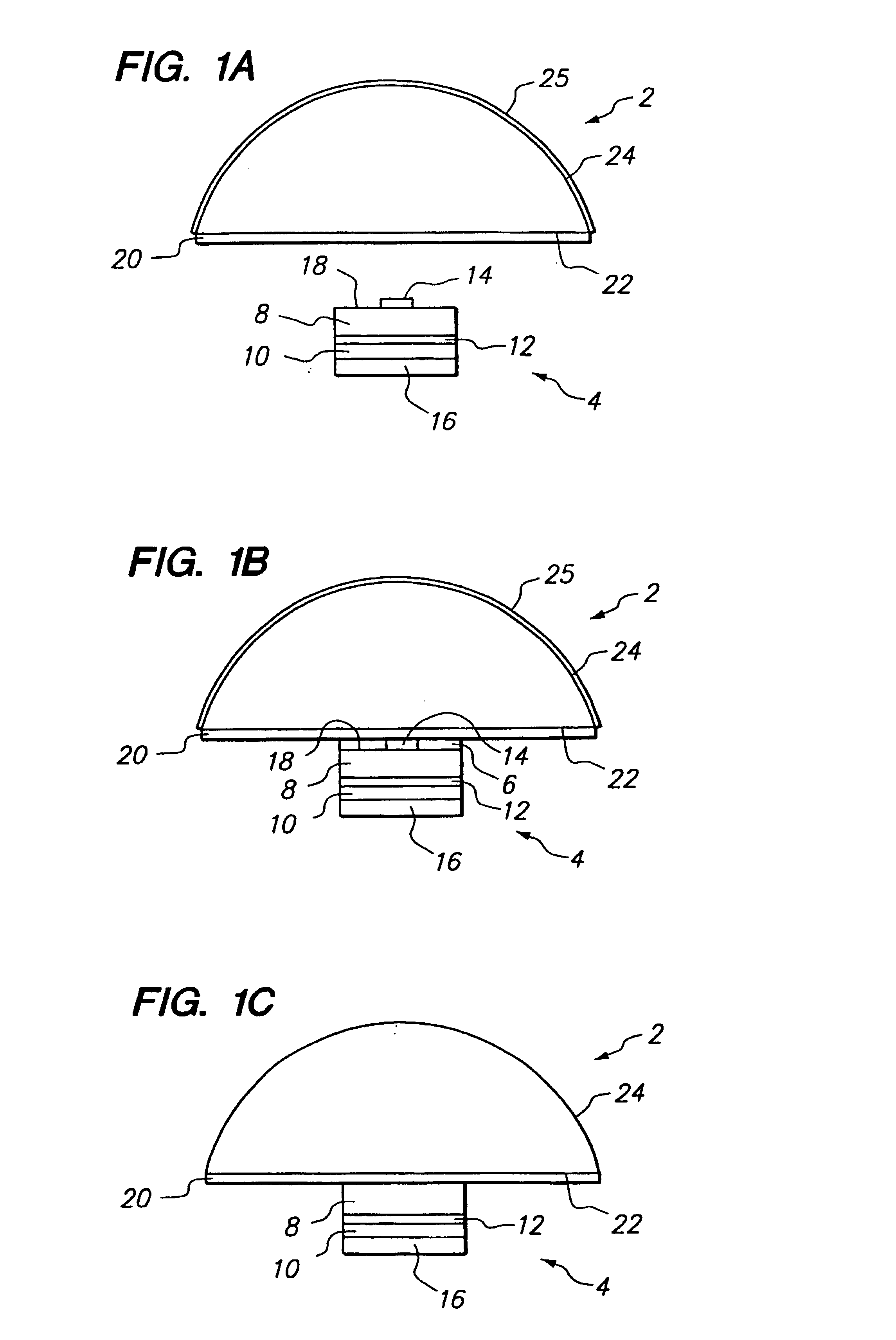
[0029]FIG. 1A depicts a transparent lens 2 and a light emitting diode (LED) die 4 to be bonded to each other in accordance with an embodiment of the present invention. In FIG. 1B, in accordance with one embodiment of the present invention, transparent lens 2 is bonded to LED die 4 with a transparent bonding layer 6.

[0030]The term “transparent” is used herein to indicate that an optical element so described, such as a “transparent lens,” a “transparent bonding layer,” a “transparent substrate,” or a “transparent superstrate” transmits light at the emission wavelengths of the LED with less than about 50%, preferably less than about 10%, single pass loss due to absorption or scattering. The emission wavelengths of the LED may lie in the infrared, visible, or ultraviolet regions of the electromagnetic spectrum. One of ordinary skill in the art will recognize that the conditions “less than 50% single pass loss” and “less than 10% single pass loss” may be met by various combinations of tr...


PUM


Abstract

Light emitting devices with improved light extraction efficiency are provided. The light emitting devices have a stack of layers including semiconductor layers comprising an active region. The stack is bonded to a transparent lens having a refractive index for light emitted by the active region preferably greater than about 1.5, more preferably greater than about 1.8. A method of bonding a transparent lens to a light emitting device having a stack of layers including semiconductor layers comprising an active region includes elevating a temperature of the lens and the stack and applying a pressure to press the lens and the stack together. Bonding a high refractive index lens to a light emitting device improves the light extraction efficiency of the light emitting device by reducing loss due to total internal reflection. Advantageously, this improvement can be achieved without the use of an encapsulant.

Description

BACKGROUND OF THE INVENTION[0001]1. Field of the Invention[0002]The present invention relates generally to light emitting devices and more particularly to light emitting diodes with enhanced light extraction efficiency.[0003]2. Description of the Related Art[0004]The light extraction efficiency of a light emitting diode (LED) is defined as the ratio of the LED's external quantum efficiency to the LED's internal quantum efficiency. Typically, the light extraction efficiency of a packaged LED is substantially less than one, i.e., much of the light generated in the LED's active region never reaches the external environment.[0005]Light extraction efficiency is reduced by total internal reflection at interfaces between the LED and surrounding material followed by reabsorption of the totally internally reflected light in the LED. For example, for a cubic geometry LED on a transparent substrate encapsulated in epoxy, the refractive index (n) at the emission wavelength changes from a value ...

Claims


Application Information

Patent Timeline
Patent Type & Authority Patents(United States)
IPC IPC(8): H01L33/00G02B3/00G02B1/00G02B3/04G02B3/08H01L33/20H01L33/50H01L33/58
CPCH01L33/58H01L33/20H01L33/505H01L2933/0058H01L33/48
Inventor CAMRAS, MICHAEL D.KRAMES, MICHAEL R.SNYDER, WAYNE L.STERANKA, FRANK M.TABER, ROBERT C.UEBBING, JOHN J.POCIUS, DOUGLAS W.TROTTIER, TROY A.LOWERY, CHRISTOPHER H.MUELLER, GERD O.MUELLER-MACH, REGINA B.
Owner LUMILEDS
Why Eureka
Try Eureka