

System for testing and burning in of integrated circuits
- Summary
- Abstract
- Description
- Claims
- Application Information
AI Technical Summary
Benefits of technology
Problems solved by technology
Method used
Image

Examples
Embodiment Construction
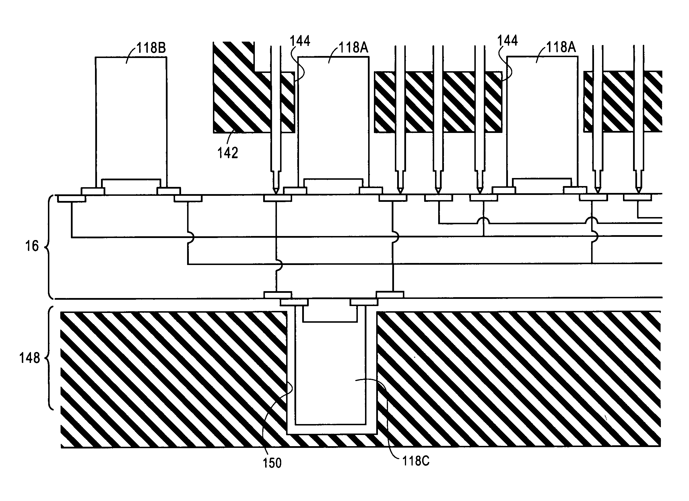
[0035]FIG. 1 of the accompanying drawings illustrates components of a contactor system 10, according to an embodiment of the invention, that is used for burn-in testing of integrated circuits 12 of an unsingulated wafer 14. The system 10 includes a power, ground reference voltage, and signal distribution board 16, a plurality of capacitors 18, and a contactor board 20. Other components such as embedded resistors, etc., that are beyond the scope of the invention are not illustrated or described herein.
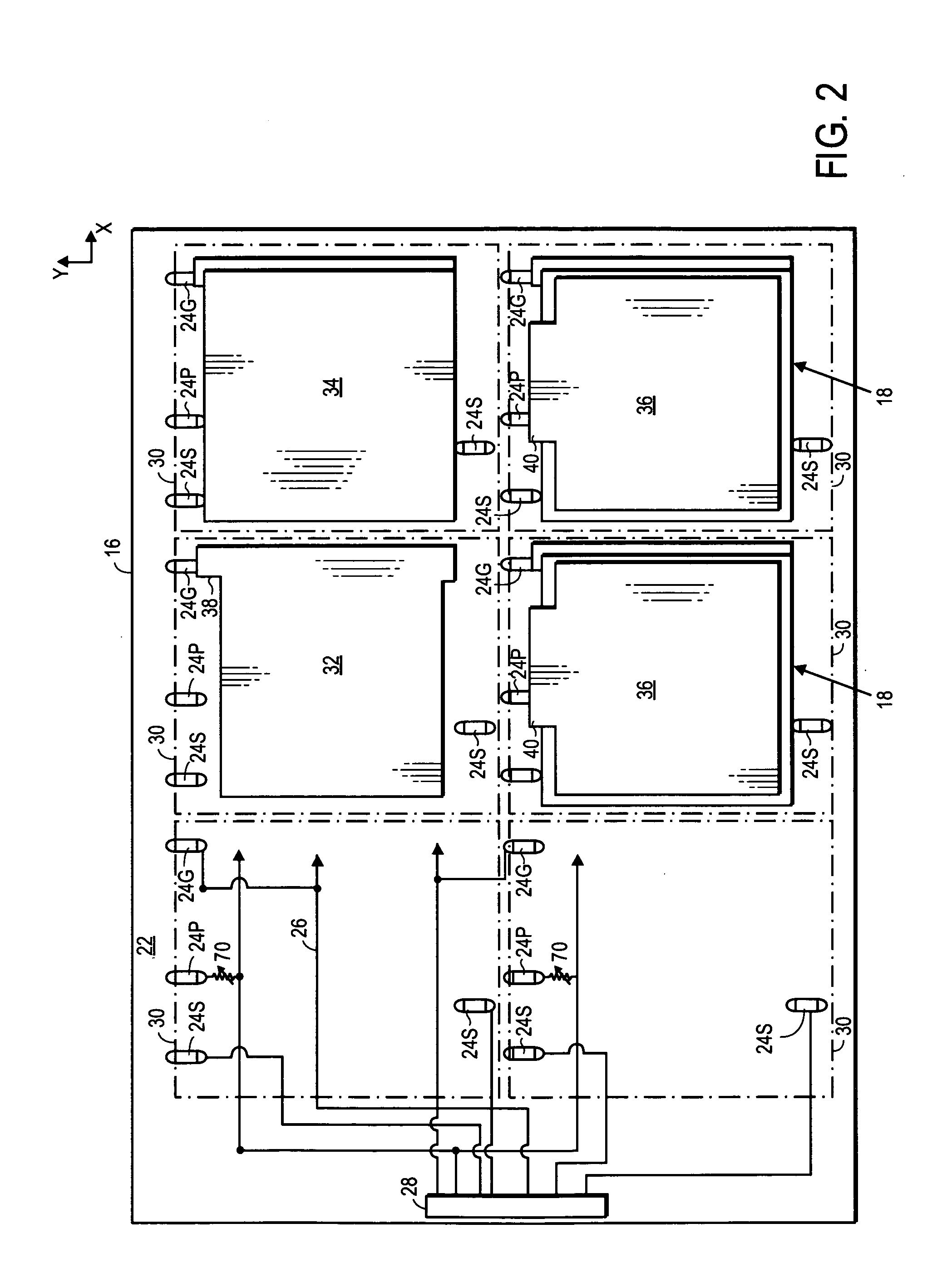
[0036]Referring to FIG. 2, the distribution board 16 includes a distribution substrate 22, a plurality of distribution board contact terminals 24, a plurality of distribution board conductors 26, and a distribution board interface 28.
[0037]The distribution substrate 22 has a plurality of regions 30. The regions 30 are in rows extending in an x-direction and columns extending in a y-direction to form an x-y array, each region 30 mirroring a respective one of the integrated circuits 12 (F...
PUM
 Abstract
Description
Claims
Application Information