Ultra low dielectric materials based on hybrid system of linear silicon precursor and organic porogen by plasma-enhanced chemical vapor deposition (PECVD)

a technology low dielectric material, which is applied in the direction of chemical vapor deposition coating, liquid surface applicator, coating, etc., can solve the problems of poor mechanical strength and failure of the integrated circui

Inactive Publication Date: 2006-06-06
APPLIED MATERIALS INC
View PDF86 Cites 58 Cited by
  • Summary
  • Abstract
  • Description
  • Claims
  • Application Information

AI Technical Summary

Benefits of technology

[0009]The present invention generally provides a method for depositing a low dielectric constant film. In one embodiment, the method includes delivering a gas mixture comprising one or more linear, oxygen-free organosilicon compounds, one or more oxygen-free hydrocarbon compounds comprising one ring and one or two carbon-carbon d

Problems solved by technology

One challenge in this area has been to develop a Si, C, and O containing film that has a low k value, but also exhibits desirable thermal and mechanical properties.
Most often, films made of a Si, C, an

Method used


Image

  • Ultra low dielectric materials based on hybrid system of linear silicon precursor and organic porogen by plasma-enhanced chemical vapor deposition (PECVD)
  • Ultra low dielectric materials based on hybrid system of linear silicon precursor and organic porogen by plasma-enhanced chemical vapor deposition (PECVD)
  • Ultra low dielectric materials based on hybrid system of linear silicon precursor and organic porogen by plasma-enhanced chemical vapor deposition (PECVD)

Examples


example 1

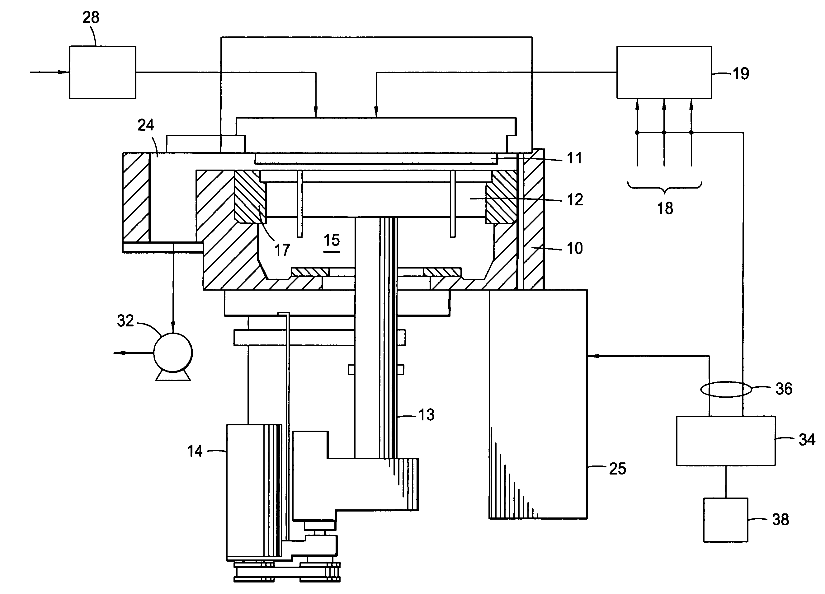
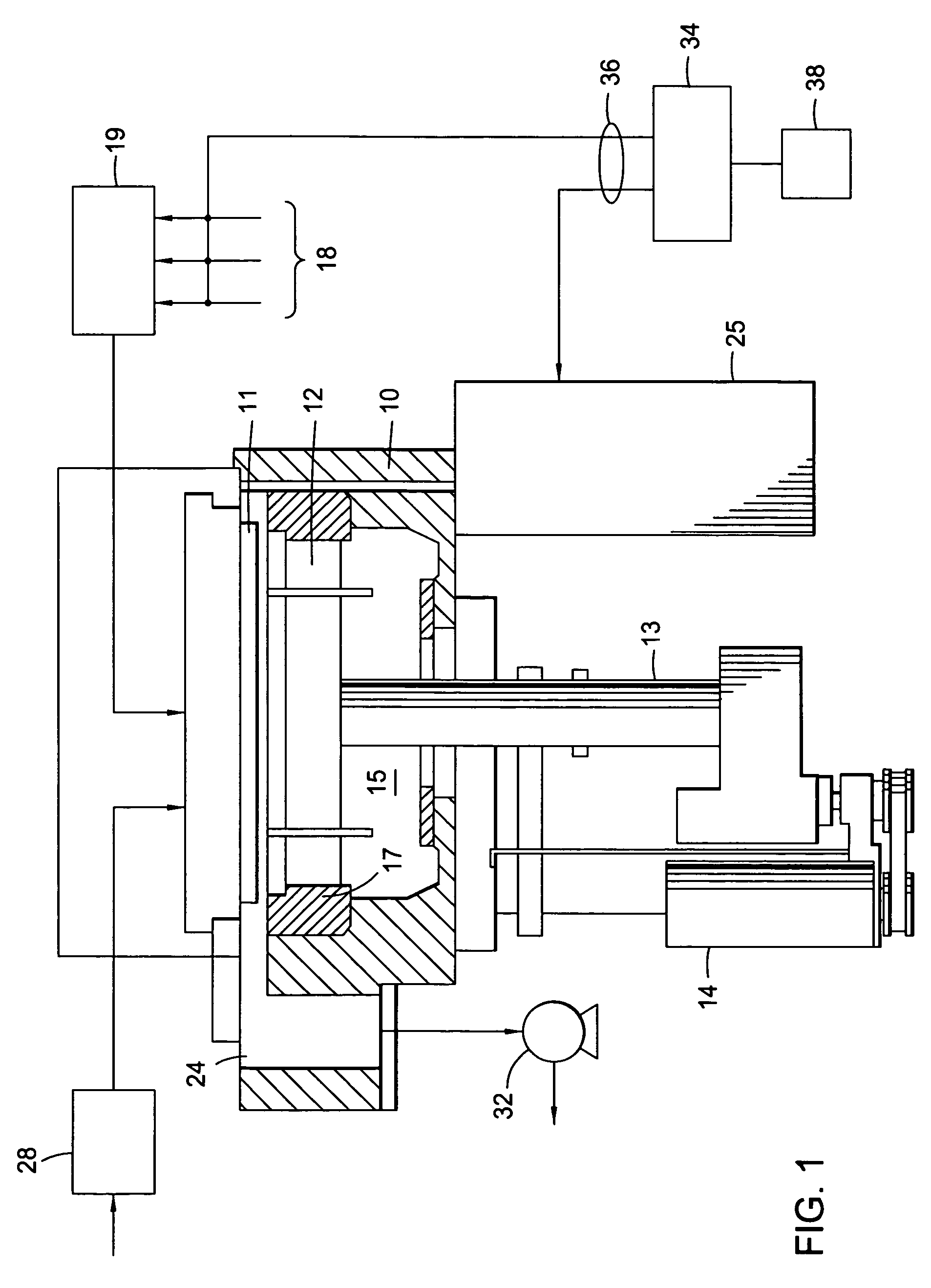
[0075]A low dielectric constant film was deposited on a 300 mm substrate at about 8 Torr and a substrate temperature of about 225° C. The following processing gases and flow rates were used:[0076]Trimethylsilane (TMS), at 1,000 sccm;[0077]Alpha-terpinene (ATP), at 3,000 mgm;[0078]Oxygen, at 200 sccm; and[0079]Helium, at 1,500 sccm.

[0080]The substrate was positioned 300 mils from the gas distribution showerhead. A power level of 600 W at a frequency of 13.56 MHz was applied to the showerhead for plasma enhanced deposition of the films. The film was deposited at a rate of about 1,000 Å / min. The film was subjected to a high temperature electron beam (e-beam) treatment using a dose of about 150 μc / cm2, at about 4.5 KeV and 1.5 mA, and at about 400° C. The e-beam treatment lasted for about 4 minutes. Following the e-beam treatment, the film exhibited a dielectric constant of about 2.5 as measured using SSM 5100 Hg CV measurement tool at 0.1 MHz. The film had a refractive index of 1.35.

example 2

[0081]A low dielectric constant film was deposited on a substrate at about 8 Torr and a temperature of about 225° C. The following processing gases and flow rates were used:[0082]Alpha-terpinene (ATP), at 3,000 mgm;[0083]Trimethylsilane (TMS), at 500 sccm;[0084]Diethoxymethylsilane (DEMS), at 600 mgm;[0085]Oxygen, at 100 sccm; and[0086]Carbon dioxide, at 1,500 sccm.

[0087]The substrate was positioned about 300 mils from the gas distribution showerhead. A power level of 600 W at a frequency of 13.56 MHz was applied to the showerhead for plasma enhanced deposition of the films. The film was deposited at a rate of about 2,000 Å / min, and had a dielectric constant (k) of about 4.3 measured using a SSM 5100 Hg CV measurement tool at 0.1 MHz. The film also exhibited a hardness of about 0.1 GPa.

E-BEAM @ 400° C. and 200 μc / cm2:

[0088]The deposited film was subjected to a high temperature electron beam (e-beam) treatment using a dose of about 200 μc / cm2, at about 4.5 KeV and 1.5 mA, and at abou...

example 3

[0089]A low dielectric constant film was deposited on a substrate at about 8 Torr and a temperature of about 225° C. The following processing gases and flow rates were used:[0090]Alpha-terpinene (ATP), at 4,000 mgm;[0091]Trimethylsilane (TMS), at 1,000 sccm;[0092]Octamethylcyclotetrasiloxane (OMCTS), at 200 mgm[0093]Oxygen, at 100 sccm; and[0094]Carbon dioxide, at 1,500 sccm.

[0095]The substrate was positioned about 300 mils from the gas distribution showerhead. A power level of 500 W at a frequency of 13.56 MHz was applied to the showerhead for plasma enhanced deposition of the films. The film was deposited at a rate of about 1,600 Å / min, and had a dielectric constant (k) of about 4.5 measured using a SSM 5100 Hg CV measurement tool at 0.1 MHz. The film also exhibited a hardness of about 0.1 GPa.

E-BEAM @ 400° C. and 200 μc / cm2:

[0096]The deposited film was subjected to a high temperature electron beam (e-beam) treatment using a dose of about 200 μc / cm2, at about 4.5 KeV and 1.5 mA, a...


PUM

PropertyMeasurementUnit
Dielectric polarization enthalpyaaaaaaaaaa

Abstract

A method for depositing a low dielectric constant film is provided by reacting a gas mixture including one or more linear, oxygen-free organosilicon compounds, one or more oxygen-free hydrocarbon compounds comprising one ring and one or two carbon-carbon double bonds in the ring, and one or more oxidizing gases. Optionally, the low dielectric constant film is post-treated after it is deposited. In one aspect, the post treatment is an electron beam treatment.

Description

CROSS-REFERENCE TO RELATED APPLICATIONS[0001]This application is a continuation-in-part of U.S. patent application Ser. No. 10 / 302,393, filed Nov. 22, 2002, which claims priority to U.S. provisional patent application Ser. No. 60 / 378,799, filed May 8, 2002, both of which are herein incorporated by reference.BACKGROUND OF THE INVENTION[0002]1. Field of the Invention[0003]The present invention relates to the fabrication of integrated circuits. More particularly, the invention relates to a method for depositing dielectric layers on a substrate and structures that include the dielectric layer.[0004]2. Description of the Related Art[0005]Semiconductor device geometries have dramatically decreased in size since such devices were first introduced several decades ago. Since then, integrated circuits have generally followed the two year / half-size rule (often called Moore's Law), which means that the number of devices that will fit on a chip doubles every two years. Today's fabrication plants...

Claims


Application Information

Patent Timeline
IPC IPC(8): C23C16/56C23C16/40C23C16/42C23C16/48H01L21/473B05D3/06B05D7/24C23C16/30H01L21/3105H01L21/312H01L21/314H01L21/768
CPCH01L21/76825C23C16/30C23C16/401C23C16/56H01L21/02126H01L21/02211H01L21/02216H01L21/02274H01L21/02351H01L21/3121H01L21/3122H01L21/7681H01L21/76814B05D1/60H01L21/31058H01L21/3125H01L21/3148B05D3/068
Inventor YIM, KANG SUBZHENG, YINEMANI, SRINIVAS D.XIA, LI-QUNHOLLAR, ERIC P.
Owner APPLIED MATERIALS INC
Why Eureka
Try Eureka