Method for manufacturing a semiconductor device that includes plasma treating an insulating film with a mixture of helium and argon gases

a technology of argon gas and insulating film, which is applied in the direction of semiconductor/solid-state device manufacturing, basic electric elements, electric apparatus, etc., can solve the problems of signal delay caused by increase of resistance of metal wirings and capacitance of interlayer insulating films, poor adhesion between different materials, and inability to obtain desired laminated structure. , to achieve the effect of suppressing the increase of leakage current and dielectric constant of the first insulating film, improving

Inactive Publication Date: 2006-06-06
RENESAS ELECTRONICS CORP
View PDF24 Cites 3 Cited by
  • Summary
  • Abstract
  • Description
  • Claims
  • Application Information

AI Technical Summary

Benefits of technology

[0012]According to the present invention, the adhesion of the first and second insulating films can be improved, a

Problems solved by technology

In recent years, as the wiring pitch has been reduced in semiconductor integrated circuits, the problem of signal delay due to increase of the resistance of metal wirings and the capacitance of interlayer insulating films has become serious.
When various materials are combined to form a multi-layer insulating film, adhesion between different materials becomes poor due to difference in the properties of the materials, and a desired laminated structure cannot be obtained.
Even if a desired laminated structure is obtained when initially formed, the multi-layer insulating film is peeled off at

Method used


Image

  • Method for manufacturing a semiconductor device that includes plasma treating an insulating film with a mixture of helium and argon gases
  • Method for manufacturing a semiconductor device that includes plasma treating an insulating film with a mixture of helium and argon gases
  • Method for manufacturing a semiconductor device that includes plasma treating an insulating film with a mixture of helium and argon gases

Examples


first embodiment

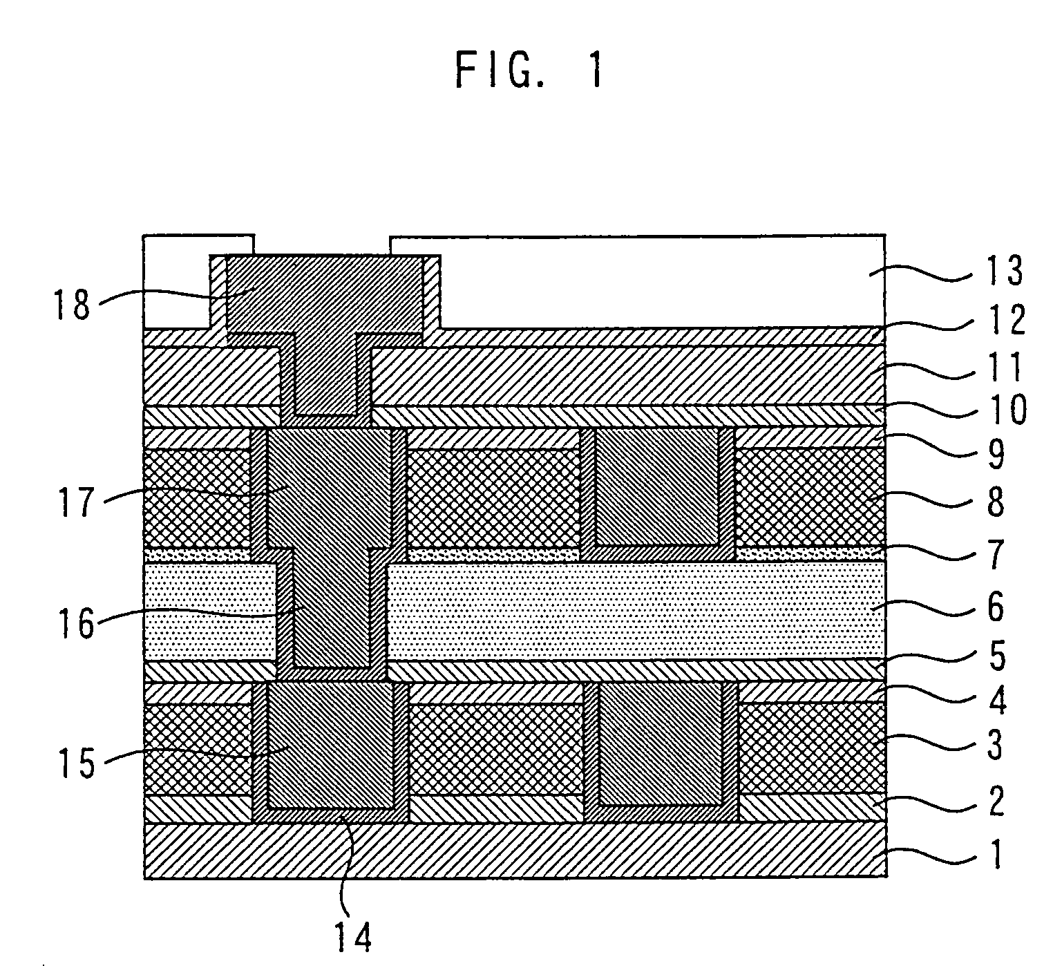
[0018]The present invention relates to a method for manufacturing a semiconductor device that has a multi-layer insulating film as an interlayer insulating film for buried Cu wirings. An example of such a multi-layer insulating film according to the present invention is shown in FIG. 1.

[0019]The multi-layer insulating film shown in FIG. 1 has, in the order from the bottom, an SiO2 film 1; an SiC film 2 of a thickness of 50 nm, which is a stopper for processing a Cu barrier and a trench; an MSQ film 3 of a thickness of 250 nm, which is an interlayer insulating film for vias and trenches; an SiO2 film 4 of a thickness of 50 nm, which is a hard mask for processing; an SiC film 5 of a thickness of 50 nm, which is a stopper for processing a Cu barrier and a trench; a fluorinated allylene film 6 of a thickness of 200 nm, which is an interlayer insulating film for vias; an adhesion promoter 7 of a film thickness of 5 to 15 nm containing a silane coupling agent; an MSQ film 8 of a thickness...

second embodiment

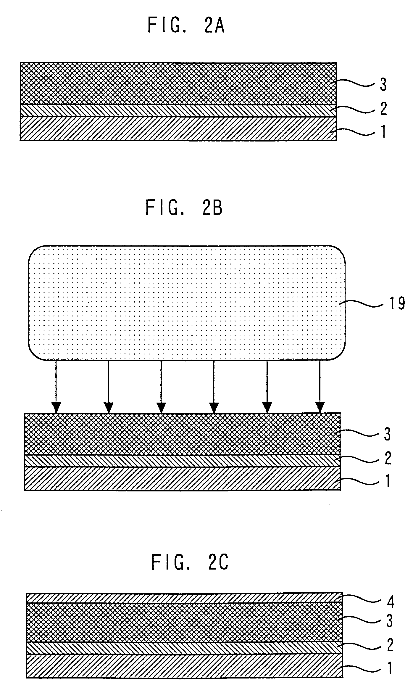
[0037]The method for manufacturing a semiconductor device according to the second embodiment of the present invention will be described below referring to FIG. 4. FIG. 4, however, shows only a part of a multi-layer insulating film shown in FIG. 1, and components such as buried Cu wirings and a substrate are not shown. The components same as the components shown in FIG. 1 will be denoted by the same reference numerals, and the description thereof will be omitted.

[0038]First, as FIG. 4A shows, in the order from the bottom, an SiC film 5 is formed using a plasma CVD method, and a fluorinated allylene film 6, which is a first insulating film, is formed using a spin coating method.

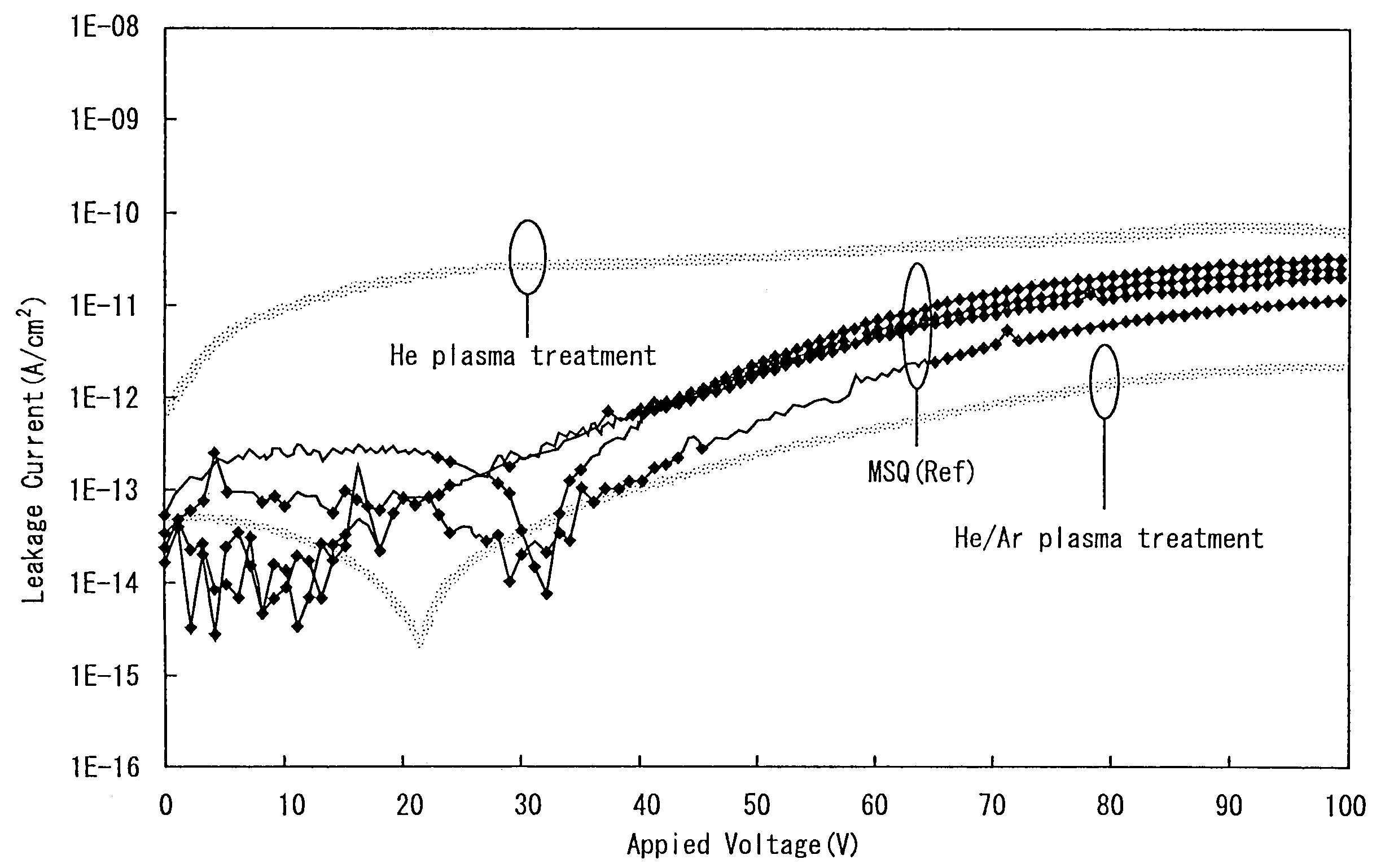
[0039]Next, as FIG. 4B shows, plasma treatment is performed on the surface of the fluorinated allylene film 6 in He / Ar mixed gas containing 5 to 31% Ar.

[0040]After the plasma treatment, as FIG. 4C shows, using the same plasma CVD chamber, an adhesion promoter 7 containing a silane coupling agent is applied onto...

third embodiment

[0042]The method for manufacturing a semiconductor device according to the third embodiment of the present invention will be described below referring to FIG. 5. FIG. 5, however, shows only a part of a multi-layer insulating film shown in FIG. 1, and components such as buried Cu wirings and a substrate are not shown. The components same as the components shown in FIG. 1 will be denoted by the same reference numerals, and the description thereof will be omitted.

[0043]First, as FIG. 5A shows, in the order from the bottom, an SiC film 5 is formed using a plasma CVD method, and a fluorinated allylene film 6, which is a first insulating film, is formed using a spin coating method. An adhesion promoter 7 containing a silane coupling agent is applied onto the fluorinated allylene film 6 using a spin coating method. Here, the film thickness of the adhesion promoter 7 is preferably 5 to 20 nm, and most preferably about 10 nm.

[0044]Next, as FIG. 5B shows, plasma treatment is performed on the ...


PUM


Abstract

In a method for manufacturing a semiconductor device having a multi-layer insulating film, a first insulating film is formed as one layer of the multi-layer insulating film, and a plasma treatment is performed on the surface of the first insulating film in an ambient of helium and argon, containing 5 to 31% Ar. After the plasma treatment, a second insulating film, different from the first insulating film, is formed on the first insulating film as another layer of the multi-layer insulating film.

Description

BACKGROUND OF THE INVENTION[0001]1. Field of the Invention[0002]The present invention relates to a method for manufacturing a semiconductor device that has a multi-layer insulating film as an interlayer insulating film for buried Cu wirings.[0003]2. Background Art[0004]In recent years, as the wiring pitch has been reduced in semiconductor integrated circuits, the problem of signal delay due to increase of the resistance of metal wirings and the capacitance of interlayer insulating films has become serious. In order to solve this problem, it has become essential to use Cu as the wiring material, and a low-dielectric-constant film (low-K film) as the interlayer insulating film. The interlayer insulating film for buried Cu wirings is formed of a multi-layer insulating film wherein a plurality of insulating films are laminated. In addition to the low-K film, the multi-layer insulating film has a Cu barrier film for preventing the diffusion of Cu from the underlying buried Cu wirings int...

Claims


Application Information

Patent Timeline
IPC IPC(8): H01L21/4757H01L21/31H01L21/3105H01L21/3205H01L21/768
CPCH01L21/31058H01L21/32056H01L21/76826H01L21/76829H01L21/76832H01L21/76835H01L21/31H01L21/3205
Inventor YONEDA, KATSUMIYOSHIE, TORU
Owner RENESAS ELECTRONICS CORP
Why Eureka
Try Eureka