Method of direct plating of copper on a ruthenium alloy

a technology of ruthenium alloy and copper, which is applied in the direction of electrical equipment, semiconductor devices, semiconductor/solid-state device details, etc., can solve the problems of insufficient seed step coverage of pvd techniques, inability to meet the demands of future interconnect technologies, and inability to fill voids of interconnect features via conventional metallization techniques. achieve the effect of reducing the critical current density and improving adhesion

Inactive Publication Date: 2006-12-21
APPLIED MATERIALS INC
View PDF39 Cites 56 Cited by
  • Summary
  • Abstract
  • Description
  • Claims
  • Application Information

AI Technical Summary

Problems solved by technology

However, as interconnect sizes decrease and aspect ratios of device features increase, void-free filling of interconnect features via conventional metallization techniques becomes increasingly difficult.
As a result thereof, conventional plating processes will likely be inadequate to support the demands of future interconnect technologies.
However, it is extremely difficult to have adequate seed step coverage with PVD techniques, as discontinuous islands of copper are often obtained close to the feature bottom in high aspect ratio features with PVD techniques.
For CVD processes, copper purity is generally questionable due to difficult complete precursor-ligand removal.
ALD techniques, though capable of giving generally conformal deposition with good adhesion to the barrier layer, suffer from very low deposition rates for depositing a continuous copper film on the sidewalls of adequate thickness to serve as a seed layer.
However, these techniques have suffered from several problems, such as adhesion failure between the copper seed layer and the barrier layer, as well as the added complexity of a complete electroless deposition system and the associated difficulties of process control.
A stress migration failure is a highly localized delamination failure that takes place in an electronic device during the thermal cycling associated with normal usage.
This thermal cycling may create voids that coalesce over time into points of failure.
Although each of these tests are somewhat qualitative, it is known in the art that deposited films that pass these tests reliably will generally not show adhesion-related problems later, such as pull-out during CMP or stress migration failures during electronic device use.
A deposited film with poor adhesion to the underlying surface will routinely fail the pull test and may even spontaneously spall off the underlying surface.
A deposited film with marginal adhesion may pass the pull test but may fail the scribe test.
Another instance of marginal film adhesion is when the film passes both the pull and scribe tests, but not reliably.
For example, the deposited film may only fail the scribe test at certain locations on the substrate, or it may only fail on intermittent substrates, or both.
Because other methods of depositing a copper seed layer onto a barrier layer are problematic, direct electroplating of a copper layer onto barrier materials has been considered.
Direct electroplating onto conventional barrier materials, such as tantalum or tantalum nitride, is difficult, since these traditional barrier materials generally have insulating native oxides across the surface.
Pre-plating treatments, such as thermal anneal in a reducing gas and cathodic reduction, have been attempted on tantalum-based barrier layers but have not improved adhesion.
Thus, adhesion of direct-electroplated copper layers is still poor on tantalum-based barrier layers that have undergone pre-plating treatments to reduce tantalum oxide present on the surface of the barrier layer.
This is because fresh tantalum surfaces are re-passivated so quickly in an aqueous electrolyte, i.e., on the order of 1 second, that adherent copper deposits cannot be obtained.

Method used


Image

  • Method of direct plating of copper on a ruthenium alloy
  • Method of direct plating of copper on a ruthenium alloy
  • Method of direct plating of copper on a ruthenium alloy

Examples


Embodiment Construction

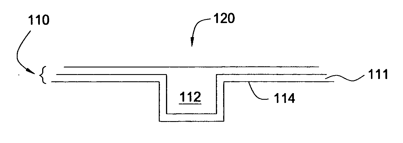
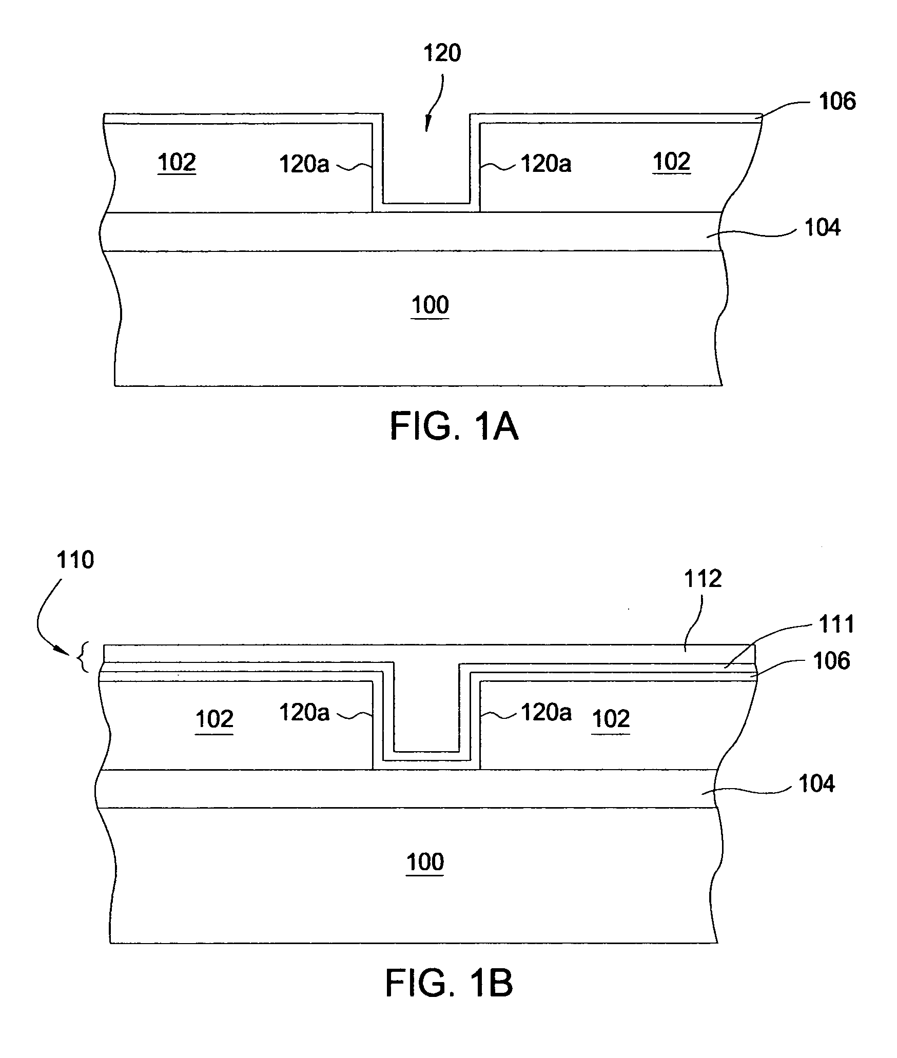
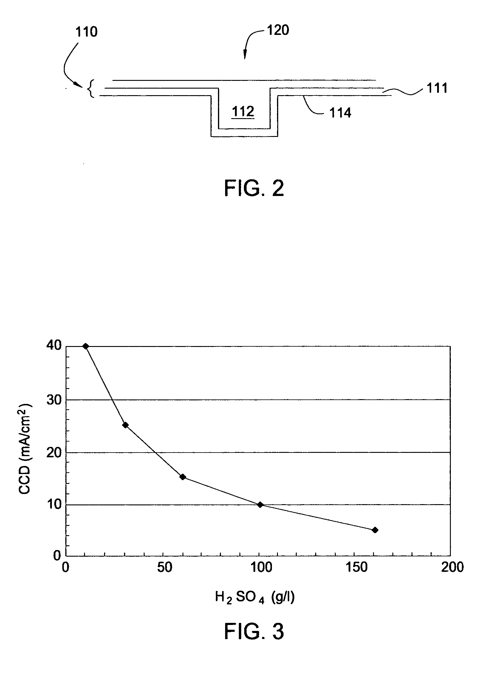
[0023] The present invention teaches a method for depositing a copper layer onto a substrate surface, generally onto a barrier layer that is an alloy of a group VIII metal and a refractory metal. A cathodic electrochemical pre-treatment or a plasma treatment may be used to condition the surface of the barrier layer prior to plating a copper layer directly onto barrier layer. The copper layer may be plated on the barrier layer in an acidic electrolyte using a nucleation voltage pulse or in an alkaline bath containing a copper complexing agent.

[0024] Ruthenium thin films, deposited by CVD, ALD or PVD, are a potential candidate for an adhesion layer between intermetal dielectric (IMD) layers and copper interconnect layers for ≦45 nm technology. Ruthenium is a group VIII metal that has a relatively low electrical resistivity (resistivity ˜7 μΩ-cm) and high thermal stability (high melting point ˜2300° C.). It is relatively stable even in the presence of oxygen and water at ambient tempe...


PUM

PropertyMeasurementUnit
concentrationaaaaaaaaaa
current densityaaaaaaaaaa

Abstract

A method is disclosed for depositing a copper seed layer onto a substrate surface, generally onto a barrier layer that is an alloy of a group VIII metal and a refractory metal. In one aspect, the alloy consists of at least 50% ruthenium and the balance a copper diffusion barrier material. A copper layer is electroplated on the alloy directly. In one aspect, the surface of the barrier layer is conditioned prior to plating to improve adhesion and reduce the critical current density for plating on the barrier layer. The conditioning may include cathodic pre-treatment or a plasma pre-treatment in a hydrogen or hydrogen / helium mixture. In one aspect, the substrate surface is immersed in an acidic plating bath and a nucleation waveform is applied to form a seed layer. In another aspect, the substrate is immersed in a neutral or alkaline copper solution that includes complexed copper ions.

Description

CROSS-REFERENCE TO RELATED APPLICATIONS [0001] This application is a continuation-in-part of co-pending U.S. patent application Ser. No. 11 / 255,368 [APPM 8241.P01], filed Oct. 21, 2005, which claims benefit of U.S. Provisional Patent Application Ser. No. 60 / 621,173 [APPM 9762L], filed Oct. 21, 2004. This application is a continuation-in-part of co-pending U.S. patent application Ser. No. 11 / 007,857 [APPM 9200], filed Dec. 9, 2004, which claims benefit of U.S. Provisional Patent Application Ser. No. 60 / 579,129, filed Jun. 10, 2004. This application is also a continuation-in-part of co-pending U.S. patent application Ser. No. 11 / 012,965 [APPM 9201], filed Dec. 15, 2004, which claims benefit of U.S. Provisional Patent Application Ser. No. 60 / 579,129, filed Jun. 10, 2004, and U.S. Provisional Patent Application Ser. No. 60 / 621,215, filed Oct. 21, 2004. This application is also a continuation-in-part of co-pending U.S. patent application Ser. No. 10 / 616,097 [APPM 8241], filed Jul. 8, 200...

Claims


Application Information

Patent Timeline
Patent Type & Authority Applications(United States)
IPC IPC(8): C25D3/38
CPCC25D3/38C25D5/10C25D5/18C25D5/34C25D5/54H01L21/2885H01L23/53238H01L21/76846H01L21/76861H01L21/76862H01L21/76868H01L21/76873H01L21/76877H01L21/76843H01L2924/0002C25D5/617H01L2924/00
Inventor HAFEZI, HOOMANROSENFELD, ARONSUN, ZHI-WENCHUNG, HUAZHU, LEI
Owner APPLIED MATERIALS INC
Why Eureka
Try Eureka