

Silicon nitride from aminosilane using PECVD
a technology of aminosilane and silicon nitride, which is applied in the direction of chemical vapor deposition coating, coating, plasma technique, etc., can solve the problems of poor hazy film with chlorine and particle contamination, less uniform film formation, and major drawbacks of using si—cl containing precursors, and achieves enhanced chemical vapor deposition, high density, and high ratio
- Summary
- Abstract
- Description
- Claims
- Application Information
AI Technical Summary
Benefits of technology
Problems solved by technology
Method used
Image

Examples
example 1
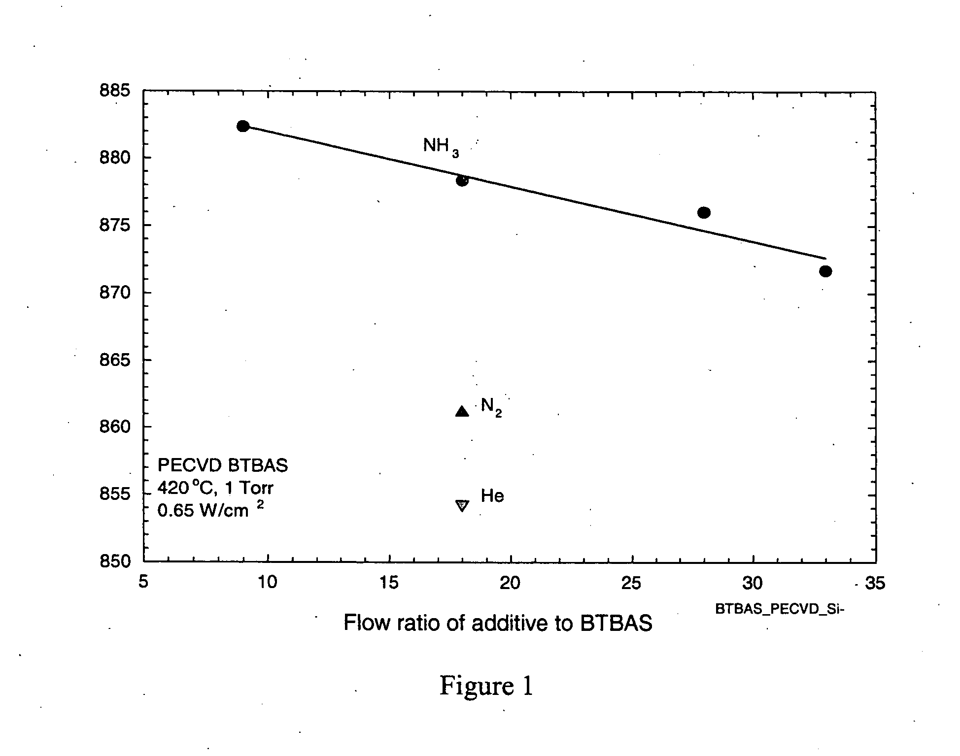
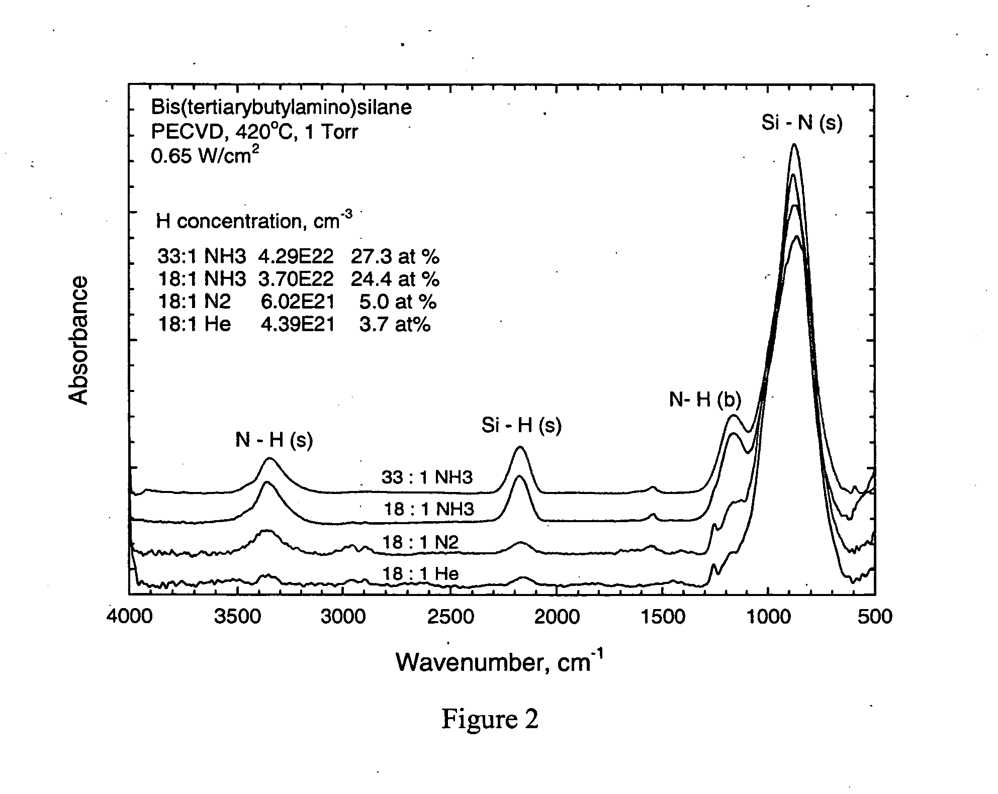
[0059] Bis(tertiarybutylamino)silane is a non-pyrophoric volatile liquid which is safer to handle than silane and dichlorosilane. The deposition process is carried out at preferably 20 mTorr-2 Torr in the temperature range of 200 to 500° C., preferably 420° C., using vapors from bis(tertiarybutylamino)silane and ammonia. Preferably, an unreactive gas diluent, such as nitrogen, helium, xenon or argon, can be used to dilute or replace the ammonia in order to achieve extremely high density silicon nitride films. The molar feed ratio of ammonia to bis(tertiarybutylamino)silane is preferably in the range of 18:1 to 33:1
[0060] The process is performed in a cold wall PECVD reaction chamber. The process steps are as follows: [0061] 1. The susceptor is maintained at approximately 420° C. [0062] 2. The silicon substrate is placed on the susceptor and sufficient time is given to reach the susceptor temperature. [0063] 3. Nitrogen or helium gas is introduced to the reaction chamber at 10 sccm....
example 2
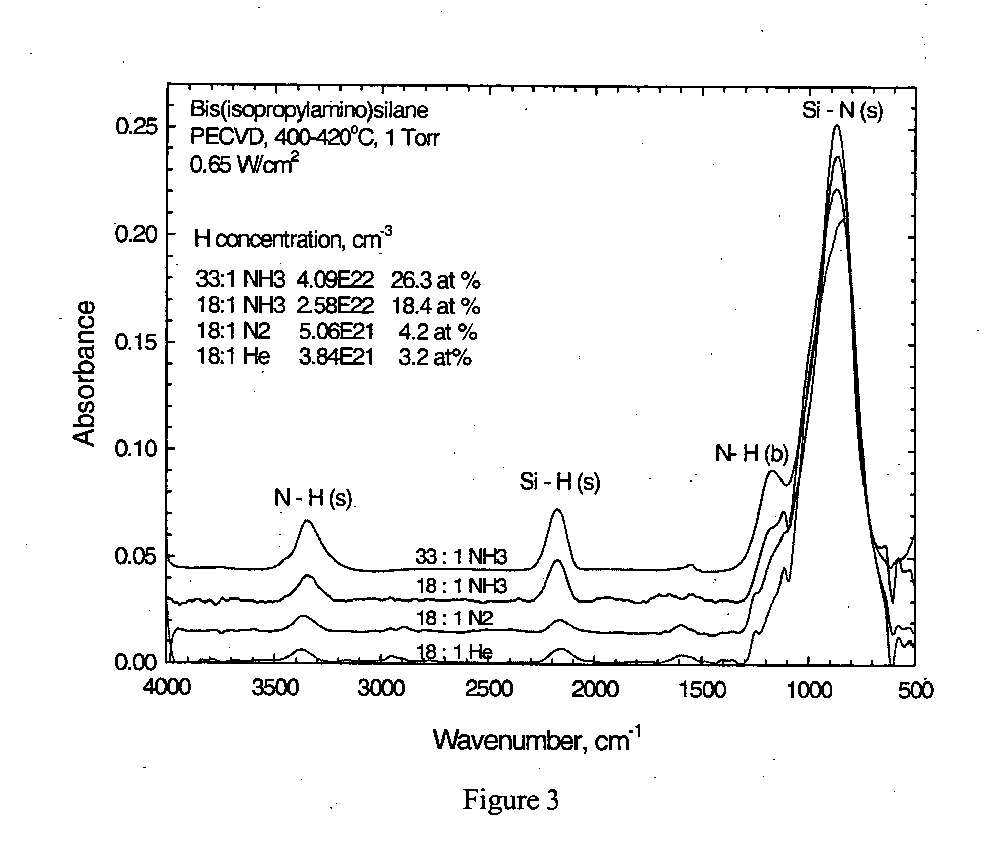
[0073] BIS(isopropylamino)silane is also non-pyrophoric volatile liquid which is safer to handle than silane and dichlorosilane. The process is identical to that in Example 1, except the precursor temperature is maintained at 40° C. because of its higher vapor pressure than BTBAS. The results of the PECVD depositions are shown in FIG. 3 under conditions given in the graph. For comparison of hydrogen concentrations, LPCVD films have approximately 3 atomic percent hydrogen. FIG. 4 shows the film stress resulting from use of different additives. The stress may be modified by different combinations of additives.
[0074] In general, silicon nitride etch resistance increases with ammonia flow contrary to LPCVD results (FIG. 5). More etch resistant and lower hydrogen concentration films are obtained by replacing ammonia with nitrogen, Significant improvements are achieved, further, by using an inert gas in place of nitrogen. Having the nitrogen in the film coming only from the aminosilane s...
PUM
| Property | Measurement | Unit |
|---|---|---|
| Temperature | aaaaa | aaaaa |
| Temperature | aaaaa | aaaaa |
| Fraction | aaaaa | aaaaa |
Abstract
Description
Claims
Application Information