
Method and system for reducing parasitic feedback and parasitic resonances in high-gain transimpedance amplifiers

a transimpedance amplifier and high-gain technology, applied in superconductive amplifiers, amplifiers with min 3 electrodes or 2 pn junctions, instruments, etc., can solve the problem of restricting the use of resistive materials to resistors, and achieve the effect of reducing parasitic feedback and resonances

Inactive Publication Date: 2006-06-06
MARVELL ASIA PTE LTD
View PDF8 Cites 2 Cited by
  • Summary
  • Abstract
  • Description
  • Claims
  • Application Information

AI Technical Summary

Benefits of technology

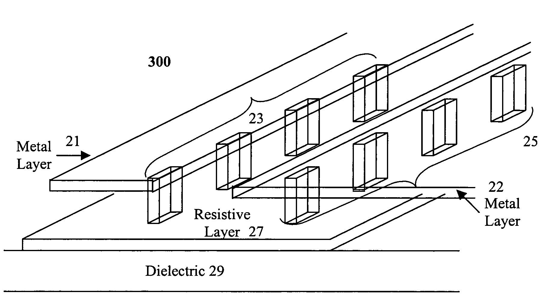
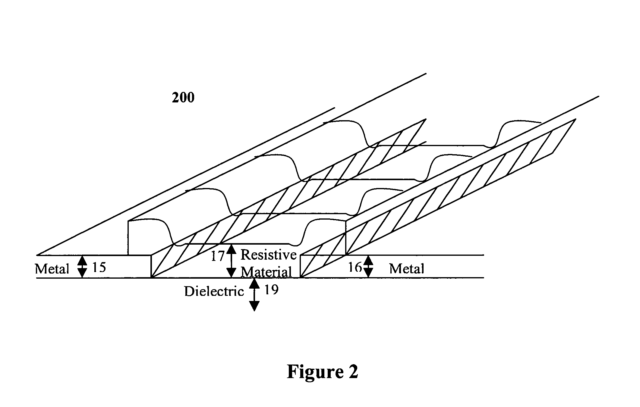
[0010]In a first embodiment of the present invention, a layer of resistive (e.g. Tantalum-Nitride, Nickel-Chrome, etc.) material is added in the gaps of a high-gain transimpedance amplifier's metal ground plane in order to reduce parasitic feedback and resonances.

Problems solved by technology

Therefore, use of resistive materials is restricted to resistors only.
Such metallic geometries in layout and packaging may form parasitic feedback paths and resonances that may turn a high-gain transimpedance amplifier into an oscillator.

Method used


Image

  • Method and system for reducing parasitic feedback and parasitic resonances in high-gain transimpedance amplifiers
  • Method and system for reducing parasitic feedback and parasitic resonances in high-gain transimpedance amplifiers
  • Method and system for reducing parasitic feedback and parasitic resonances in high-gain transimpedance amplifiers

Examples


Embodiment Construction

[0019]The following description is presented to enable one of ordinary skill in the art to make and use the invention and is provided in the context of a patent application and its requirements. In the following description, specific nomenclature is set forth to provide a thorough understanding of the present invention. It will be apparent to one skilled in the art that the specific details may not be necessary to practice the present invention. Furthermore, various modifications to the embodiments will be readily apparent to those skilled in the art and the generic principles herein may be applied to other embodiments. Thus, the present invention is not intended to be limited to the embodiments shown but is to be accorded the widest scope consistent with the principles and features described herein.

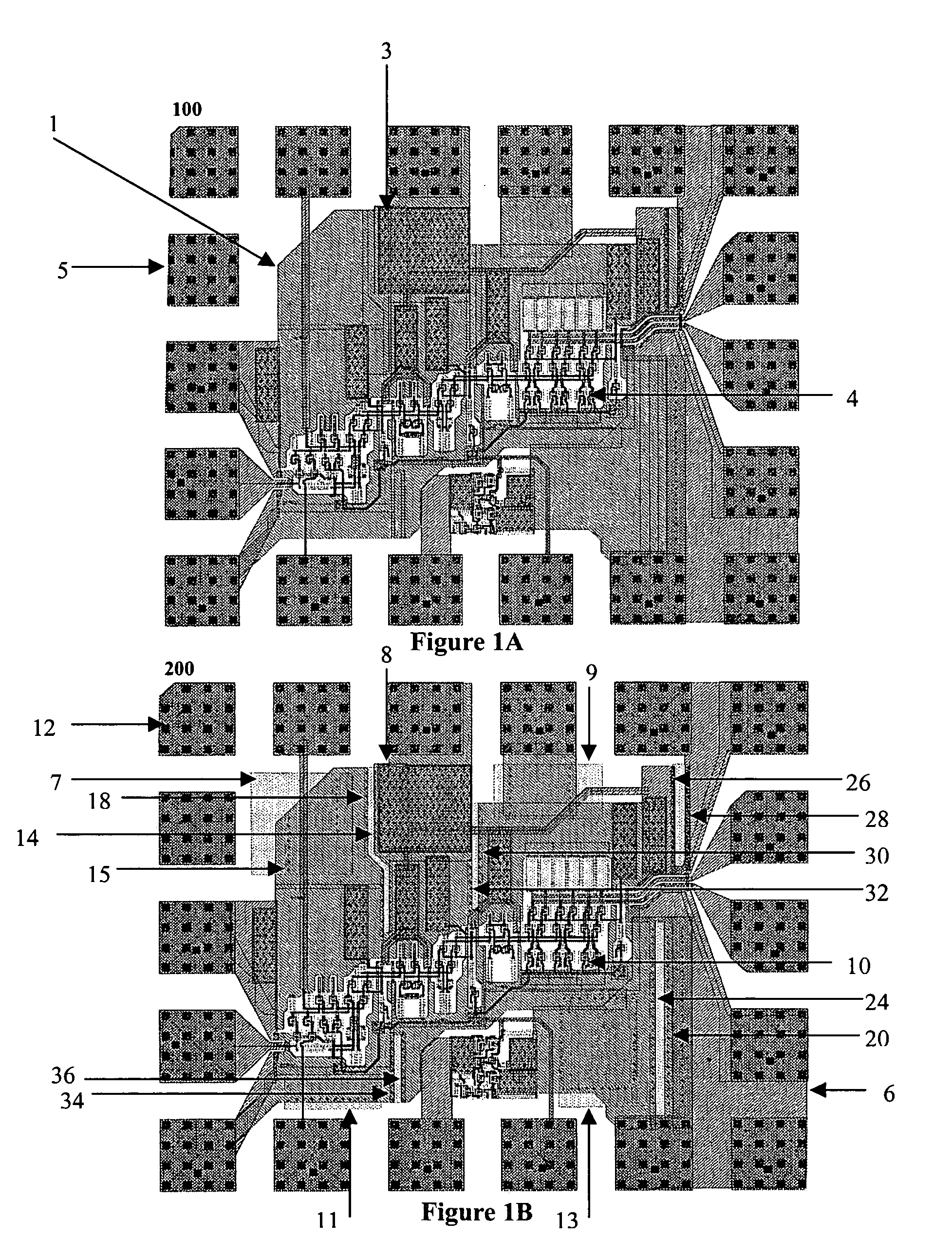
[0020]FIG. 1B illustrates a schematic diagram 200 of a high-gain transimpedance amplifier in accordance to one embodiment of the present invention. Schematic diagram 200 comprises: a gro...


PUM


Abstract

Method and system for reducing parasitic feedback and resonances in high-gain transimpedance amplifiers. In a first embodiment of the present invention, a resistive layer is implemented in the gaps of a high-gain transimpedance amplifier's metallic planes. In a second embodiment of the present invention, a resistive layer is implemented underneath a high-gain transimpedance amplifier's ground plane, vias are implemented to create contact between the resistive layer and the ground plane.

Description

BACKGROUND INFORMATION[0001]1. Field of Invention[0002]The present invention relates to transimpedance amplifiers, and more particularly, to high-gain transimpedance amplifiers with reduced parasitic feedback and resonances.[0003]2. Description of Related Art[0004]A transimpedance amplifier is used to convert an input current to a proportional output voltage. A typical transimpedance amplifier comprises: an input current that is supplied through a transistor input stage, the input current is typically produced by a photodiode; an output carrying an output voltage; and a coupling member connecting the input to the output. Furthermore, the input current may be small, such as 1 μA, or comparatively large, such as 1 mA.[0005]Typical uses of transimpedance amplifiers include summing currents as part of a frequency impulse response filter or processing reverse current produced by a photodiode as function of infrared signal energy received by the photodiode.[0006]FIG. 1A illustrates a layo...

Claims


Application Information

Patent Timeline
IPC IPC(8): H03F19/00
CPCH03F3/08
Inventor BROEKAERT, TOM PETER EDWARDPOSPIESZALSKI, MARIAN
Owner MARVELL ASIA PTE LTD
Learn More