Method for forming ultra low k films using electron beam

a technology of electron beam and ultra-low k, applied in the direction of electric heating, vacuum evaporation coating, coating, etc., can solve the problems of mechanical strength and failure of the integrated circui

Inactive Publication Date: 2006-06-13
APPLIED MATERIALS INC
View PDF75 Cites 41 Cited by
  • Summary
  • Abstract
  • Description
  • Claims
  • Application Information

AI Technical Summary

Problems solved by technology

One challenge in this area has been to develop a Si, C, and O containing film that has a low k value, but also exhibits desirable thermal and mechanical properties.
Most often, films made of a Si, C, and O network that have a desirable dielectric constant exhibit poor mechanical strength and are easily damaged by etch chemistry and subsequent plasma exposure, causing failure of the integrated circuit.

Method used


Image

  • Method for forming ultra low k films using electron beam
  • Method for forming ultra low k films using electron beam
  • Method for forming ultra low k films using electron beam

Examples


example 1

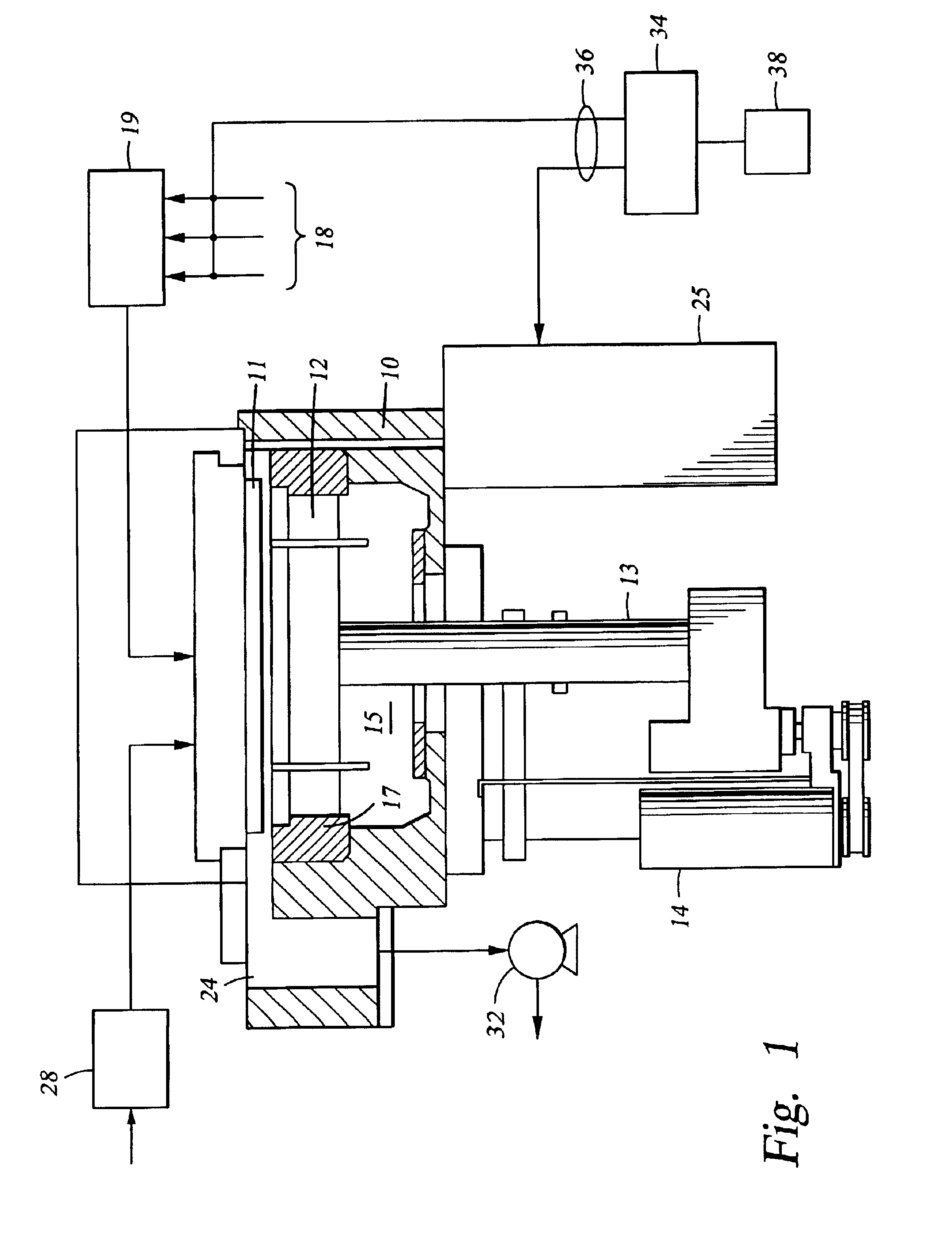
[0070]A low dielectric constant film was deposited on each of three 200 mm substrates at about 8 Torr and temperature of about 200° C. The following processing gases and flow rates were used:

[0071]Alpha-terpinene (ATP), at 3,000 mgm;

[0072]Diethoxymethylsilane (DEMS), at 800 mgm; and

[0073]Carbon dioxide, at 1,000 sccm.

[0074]Each substrate was positioned 300 mils from the gas distribution showerhead. A power level of 600 W at a frequency of 13.56 MHz was applied to the showerhead for plasma enhanced deposition of the films. Each film was deposited at a rate of about 2,700 Å / min, and had a dielectric constant (k) of about 5.4 measured using a SSM 5100 Hg CV measurement tool at 0.1 MHz. Each film also exhibited a hardness of about 0.1 GPa.

Thermal Anneal:

[0075]The first deposited film was subjected to a thermal anneal process. The anneal treatment utilized a temperature of about 425° C. at a pressure of about 10 Torr in an inert gas environment for about 4 hours. Shorter anneal times res...

example 2

[0078]A low dielectric constant film was deposited on each of three substrates at about 8 Torr and temperature of about 225° C. The following processing gases and flow rates were used:

[0079]Alpha-terpinene (ATP), at 3,000 mgm;

[0080]Diethoxymethylsilane (DEMS), at 800 mgm;

[0081]Carbon dioxide, at 1,500 sccm; and

[0082]Oxygen, at 100 sccm.

[0083]Each substrate was positioned 300 mils from the gas distribution showerhead. A power level of 600 W at a frequency of 13.56 MHz was applied to the showerhead for plasma enhanced deposition of the films. Each film was deposited at a rate of about 1,800 A / min, and had a dielectric constant (k) of about 2.85 measured using SSM 5100 Hg CV measurement tool at 0.1 MHz. Each film also exhibited a hardness of about 0.23 GPa.

Thermal Anneal:

[0084]The first deposited film was subjected to a thermal anneal process. The anneal treatment utilized a temperature of about 450° C. at a pressure of about 10 Torr in an inert gas environment for about 30 minutes. Sh...

example 3

[0087]A low dielectric constant film was deposited on each of two substrates at about 8 Torr and a temperature of about 225° C. The following processing gases and flow rates were used:

[0088]Alpha-terpinene (ATP), at 4,000 mgm;

[0089]Octamethylcyclotetrasiloxane (OMCTS), at 200 mgm;

[0090]Oxygen, at 200 sccm; and

[0091]Carbon dioxide 2,000 sccm.

[0092]Each substrate was positioned about 300 mils from the gas distribution showerhead. A power level of 500 W at a frequency of 13.56 MHz was applied o the showerhead for plasma enhanced deposition of the films. Each film was deposited at a rate of about 1,000 Å / min, and had a dielectric constant (k) of about 4.0 measured using a SSM 5100 Hg CV measurement tool at 0.1 MHz. Each film also exhibited a hardness of about 0.1 GPa.

E-BEAM @ 400° C. and 120 μc / cm2:

[0093]The first deposited film was subjected to a high temperature electron beam (e-beam) treatment using a dose of about 120 μc / cm2, at about 4.5 KeV and 1.5 mA, and at about 400° C. The e-b...


PUM

PropertyMeasurementUnit
dielectric constantaaaaaaaaaa
pressureaaaaaaaaaa
temperatureaaaaaaaaaa

Abstract

The present invention generally provides a method for depositing a low dielectric constant film using an e-beam treatment. In one aspect, the method includes delivering a gas mixture comprising one or more organosilicon compounds and one or more hydrocarbon compounds having at least one cyclic group to a substrate surface at deposition conditions sufficient to deposit a non-cured film comprising the at least one cyclic group on the substrate surface. The method further includes substantially removing the at least one cyclic group from the non-cured film using an electron beam at curing conditions sufficient to provide a dielectric constant less than 2.5 and a hardness greater than 0.5 GPa.

Description

BACKGROUND OF THE INVENTION[0001]1. Field of the Invention[0002]The present invention relates to the fabrication of integrated circuits. More particularly, the invention relates to a method for depositing dielectric layers on a substrate and the structures formed by the dielectric layer.[0003]2. Description of the Related Art[0004]Semiconductor device geometries have dramatically decreased in size since such devices were first introduced several decades ago. Since then, integrated circuits have generally followed the two year / half-size rule (often called Moore's Law), which means that the number of devices that will fit on a chip doubles every two years. Today's fabrication plants are routinely producing devices having 0.13 μm and even 0.1 μm feature sizes, and tomorrow's plants soon will be producing devices having even smaller geometries.[0005]In order to further reduce the size of devices on integrated circuits, it has become necessary to use conductive materials having low resis...

Claims


Application Information

Patent Timeline
Patent Type & Authority Patents(United States)
IPC IPC(8): C23C16/56B05D3/06B05D7/24C23C16/40H01L21/3105H01L21/312
CPCC23C16/401C23C16/56H01L21/02126H01L21/02216H01L21/7681H01L21/02351H01L21/3122H01L21/02274B05D1/60B05D3/068H01L21/31058H01L21/3121H01L21/3125
Inventor ZHENG, YINEMANI, SRINIVAS D.XIA, LI-QUNHOLLAR, ERICYIM, KANG SUB
Owner APPLIED MATERIALS INC
Why Eureka
Try Eureka