Semiconductor integrated circuit

a semiconductor and integrated circuit technology, applied in the field of digital/analog mixed type semiconductor integrated circuits, can solve the problems of difficult to predict the optimum clock phase difference, adversely affecting the operation of the analog circuit via the semiconductor substrate, and causing noise, so as to ensure the minimization of the noise component of the analog circui

Inactive Publication Date: 2006-06-13
SHARP KK
View PDF12 Cites 9 Cited by
  • Summary
  • Abstract
  • Description
  • Claims
  • Application Information

AI Technical Summary

Benefits of technology

[0011]Accordingly, an object of the present invention is to provide a semiconductor integrated circuit capable of adjusting clock phases to a digital circuit so that a noise component of a analog circuit is always minimized even when variation occurs in transistor characteristics, resistance or the like during manufacturing.
[0019]According to the above constitution, the phase shift circuit for minimizing a noise component generated by the analog circuit is obtained out of a plurality of phase shift circuits by operations of selection control means and phase shift setting means. Then, only the aforementioned phase shift circuit is fixedly selected and the subsequent phase shift value is set. Therefore, even when variation in transistor characteristics or resistance occurs in semiconductor integrated circuits in the manufacturing stage, the noise component generated by the analog circuit is minimized thereafter.
[0027]According to the above constitution, a phase shift value minimizing the noise component is repeatedly set at intervals of the second specified time. Therefore, even when a variation in a phase shift value set when the first specified time elapses after having powered on occurs due to a temperature rise or a change in a power source voltage during the operation period, a noise component generated by the analog circuit is always minimized.

Problems solved by technology

In such a digital / analog mixed type semiconductor integrated circuit, there is a problem that digital noises generated upon an operation of the digital circuit adversely affect an operation of the analog circuit via a power source, ground, substrate or the like.
Then, this change adversely affects an operation of the analog circuit via the semiconductor substrate and produces noises.
When the clock phases are to be shifted, however, it is very difficult to predict an optimum clock phase difference before designing since a shift amount of the clock phases is changed in practice by a wiring resistance, stray capacitance or the like within a device.
In the conventional semiconductor integrated circuit device, however, there are problems described below.
Therefore, that clock phase difference generating circuits which are the same on design do not always generate a constant clock phase difference.
Therefore, in the above-described semiconductor integrated circuit device, a clock phase difference generating circuit producing the least noise components is not always selected.

Method used


Image

  • Semiconductor integrated circuit
  • Semiconductor integrated circuit
  • Semiconductor integrated circuit

Examples


first embodiment

(First Embodiment)

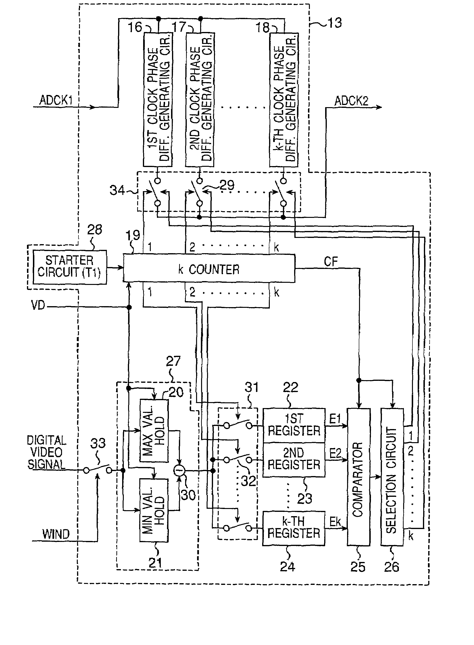
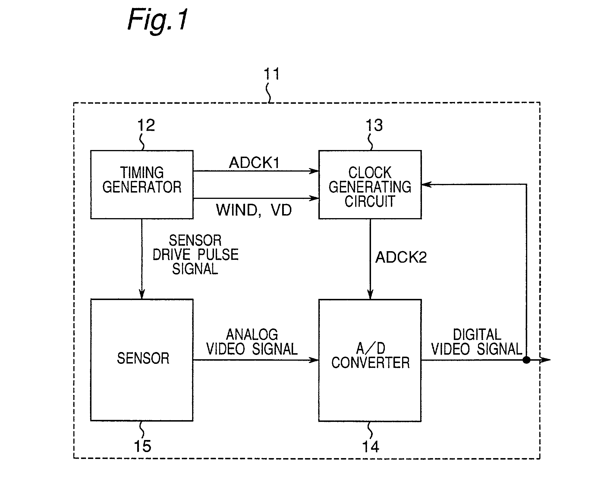
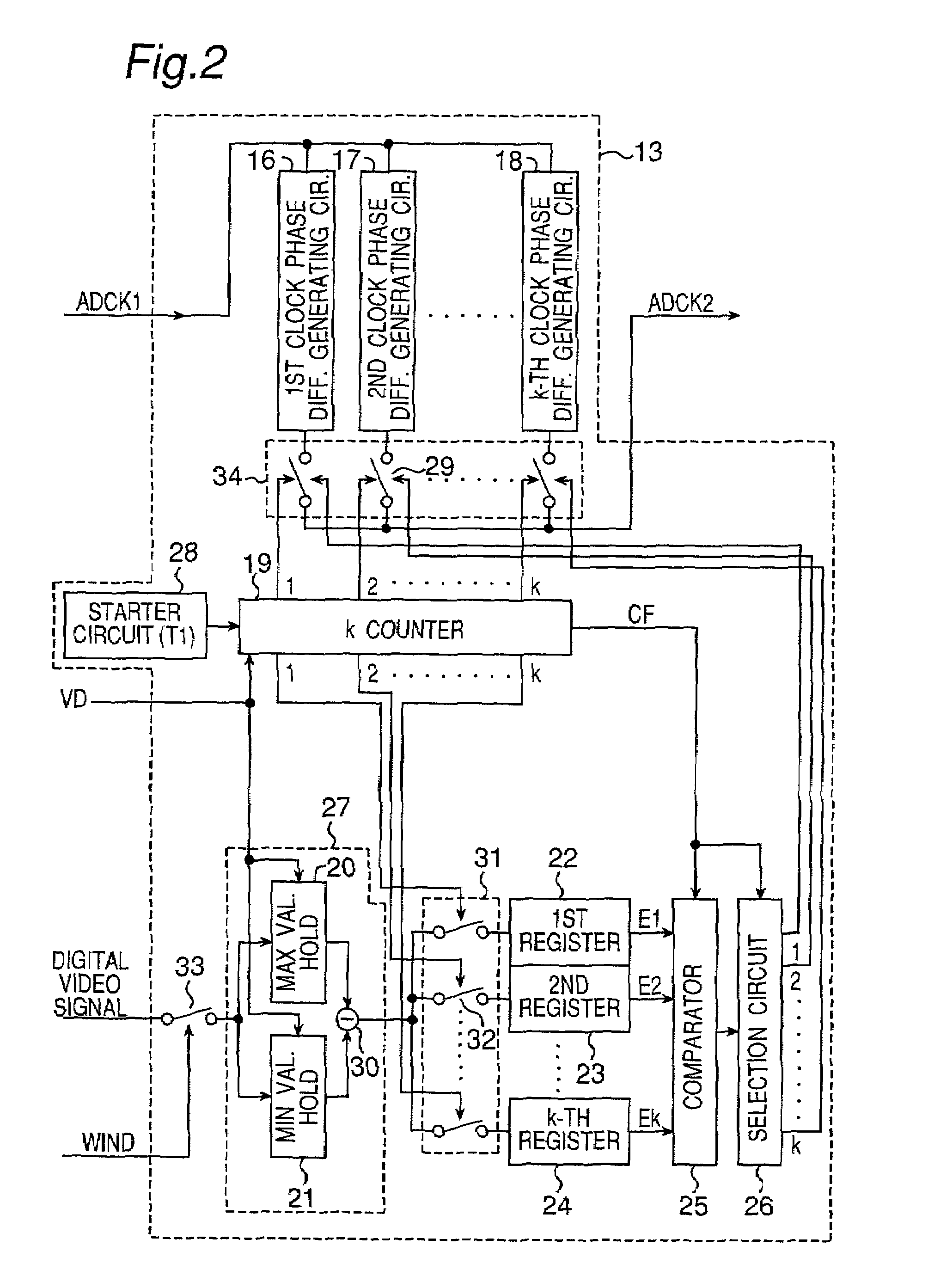
[0040]FIG. 1 is a block diagram of a semiconductor integrated circuit of this embodiment. This semiconductor integrated circuit 11 is an integrated circuit which is an A / D converter-incorporated CMOS-type solid-state image sensing device. This integrated circuit includes a clock generating circuit 13 generating a clock signal ADCK2 obtained by shifting a phase of a basic clock signal ADCK1 for driving the A / D converter 14 outputted from a timing generator 12 to a phase for minimizing a noise component included in an output signal of the A / D converter 14. An analog video signal from each solid-state image sensing element of a sensor 15 driven in response to a sensor drive pulse signal (having the same period as that of the basic clock signal ADCK1) from the timing generator 12 is A / D-converted by the A / D converter 14 to output a digital video signal.

[0041]That is, in this embodiment, the sensor drive pulse signal is an example of a first clock signal. The sensor 15 ...

second embodiment

(Second Embodiment)

[0052]The configuration of the clock generating circuit 13 in FIG. 1 is not limited to the one shown in FIG. 2. This embodiment relates to another circuit configuration of the clock generating circuit 13.

[0053]FIG. 4 is a block diagram showing a configuration of the clock generating circuit 13 in FIG. 1 different from the first embodiment. In FIG. 4, a first to k-th clock phase difference generating circuits 41–43, switch group 44, starter circuit 45, k counter 46, switch 47, switch group 51, first to k-th registers 52–54, comparator 55 and selection circuit 56 have the same constitutions as those of the first to k-th clock phase difference generating circuits 16–18, switch group 34, starter circuit 28, k counter 19, switch 33, switch group 31, first to k-th registers 22–24, comparator 25 and selection circuit 26, respectively, in the above first embodiment shown in FIG. 2.

[0054]In this embodiment, measurement of a noise component included in a digital video signa...

third embodiment

(Third Embodiment)

[0057]As described in the above second embodiment, various methods are considered as a method for measuring the noise component. However, a temperature may rise or a power source voltage may change in an operation period of the clock generating circuit 13. In such a case, transistor characteristics change even in the first or second embodiment. Therefore, there are cases where a clock phase difference generating circuit selected in an initial stage of the operation is not necessarily an optimum clock phase difference generating circuit.

[0058]This embodiment relates to a clock generating circuit which can deal with such a case. In a case of the clock generating circuit 13 in the first or second embodiment, the power source is inputted, the operation is stabilized, and then the optimum clock phase difference generating circuit is selected only in the k V periods in the initial stage. On the other hand, in a case of the clock generating circuit in this embodiment, the...


PUM


Abstract

Even when variation in transistor characteristic, resistance or the like occurs during manufacturing, a noise component is always minimized. Each of k clock phase difference generating circuits 16–18 shifts a phase of a basic clock signal ADCK1 by a specified different value to obtain a clock signal ADCK2 and supplies the clock signal ADCK2 to an A / D converter. A k counter 19 successively selects the clock phase difference generating circuits 16–18 and stores a noise component in an output of the A / D converter measured by a noise measuring circuit 27 in a corresponding register. A comparator 25 compares k noise components and obtains the number j of the clock phase difference generating circuit giving a minimum value. A selection circuit 26 fixedly selects only the j-th clock phase difference generating circuit. Thus, even when variation in the transistor characteristics or resistance occurs in each device in a manufacturing stage, the clock signal ADCK2 obtained by shifting the phase of the basic clock signal ADCK1 can be supplied to the A / D converter so that a noise component is minimized for each device.

Description

BACKGROUND OF THE INVENTION[0001]The present invention relates to a digital / analog mixed type semiconductor integrated circuit wherein a digital circuit and analog circuit are formed on the same semiconductor substrate. In particular, the present invention relates to a digital / analog mixed type semiconductor integrated circuit such as a CMOS (complementary metal oxide semiconductor)-type solid-state image sensing device or the like which incorporates a digital signal processing circuit and an A / D (Analog / Digital) converter and handles weak analog signals.[0002]With a more highly integrated semiconductor circuit, the system-on-chip method, in which one system is formed on the same substrate, is being used more widely. A digital / analog mixed type semiconductor integrated circuit is also being used wherein a digital circuit and an analog circuit often provided on separate chips conventionally are formed on the same substrate.[0003]In such a digital / analog mixed type semiconductor integ...

Claims


Application Information

Patent Timeline
IPC IPC(8): H04N5/217G01R29/02H03K19/096H03K9/08H04N3/14H04N5/335G01R29/00H01L27/146H01L21/822H01L27/04H03K19/00H03L7/00H03M1/08H04N5/232H04N5/357H04N5/369H04N5/378
CPCH03M1/08H04N5/335H04N3/1562H04N3/155H04N25/617H04N25/7795H03L7/00H04N25/00H04N25/745
Inventor KOYAMA, EIJI
Owner SHARP KK
Why Eureka
Try Eureka