Printing device and method of manufacturing a light emitting device

a printing device and light-emitting technology, which is applied in the direction of inking apparatus, identification means, instruments, etc., can solve the problems of loss, inability to heat-resistance or water-resistance organic compound layer formation, and loss of organic compound material that remains on the inner wall of the evaporation device and in the crucible of the evaporation source, so as to achieve increased printing speed and shorten the time for position control. , the effect o

Inactive Publication Date: 2006-06-20
SEMICON ENERGY LAB CO LTD
View PDF12 Cites 12 Cited by
  • Summary
  • Abstract
  • Description
  • Claims
  • Application Information

AI Technical Summary

Benefits of technology

[0012]The present invention has been made in view of the above-described problems, and an object of the present invention is therefore to provide a printing device which is capable of conducting formation of an organic compound layer by an ink jet method in a simple and easy manner and at high speed, and to provide a method of manufacturing a light emitting device using the printing device.
[0015]A solution in which an organic fight emitting material or a precursor thereof is dissolved or dispersed in a liquid is used as the mixture. The mixture is discharged continuously, whereby the time for position control is shortened and the printing speed can be increased in comparison with an ink jet method in which ink is printed for each dot. In particular, the present invention is appropriately applied to a production method using mother glass, in which a plurality of display panels are taken out from a large-area substrate. Further, in the case where a plurality of pixel regions are provided in the mother glass, the discharge of the mixture is stopped instantaneously during a movement of the ink head between the pixel regions, whereby the ink head can be moved at higher speed to the mother glass. The second piezoelectric element is provided in order to stop the discharge of the mixture instantaneously, whereby the high speed in printing can be realized.
[0019]The first and second piezoelectric elements are incorporated into the ink head, and the timings for causing displacement are synchronized, whereby the mixture can be discharged continuously, or the discharge can be stopped instantaneously. The mixture is discharged continuously to form an organic compound layer. Thus, the time for position control is shortened, and the printing speed can be increased in comparison with an ink jet method in which ink is printed for each dot. In particular, the present invention is appropriately applied to a production method in which a plurality of display panels are taken out from a large-area substrate. Further, in the case where a plurality of pixel regions are provided in the large-area substrate, the discharge of the mixture is stopped instantaneously during a movement of the ink head between the pixel regions, whereby the ink head can be moved at higher speed to the large-area substrate. The second piezoelectric element is provided in order to stop the discharge of the mixture instantaneously. This means is provided, whereby the high speed in printing can be realized.

Problems solved by technology

It is impossible in terms of heat-resistance or water-resistance that an organic compound layer is formed by patterning with an exposure process like semiconductor.
In this case, an organic compound material attached to the shadow mask is not utilized and lost.
Besides, the organic compound material that remains on an inner wall of a chamber of an evaporation device and in a crucible of an evaporation source becomes a loss.
Therefore, the low molecular weight organic compound layer formed by the vacuum evaporation method has involved a problem in that the utilization efficiency of the material is poor.
However, the low molecular weight organic compound material needed to have higher purity is expensive, which is reflected in the cost of a product.
However, as a multiple production method in which a plurality of display panels are taken out from one large-area substrate, it can not be said that the ink jet method in which a mixture is dropped each dot has always high capacity as an effective production method.
The ink jet method has involved a problem in that a processing time increases after all since higher accuracy of position and higher processing speed are demanded as a screen size becomes larger and the number of pixels increases.
Further, in the case where the organic compound layer is formed by dropping the mixture every dot, variation in a discharge amount of the mixture and fluctuation of a drop position lead to unevenness in emission intensity, which causes degradation of quality of a light emitting device constituted of a large number of light emitting elements.

Method used


Image

  • Printing device and method of manufacturing a light emitting device
  • Printing device and method of manufacturing a light emitting device
  • Printing device and method of manufacturing a light emitting device

Examples


embodiment 1

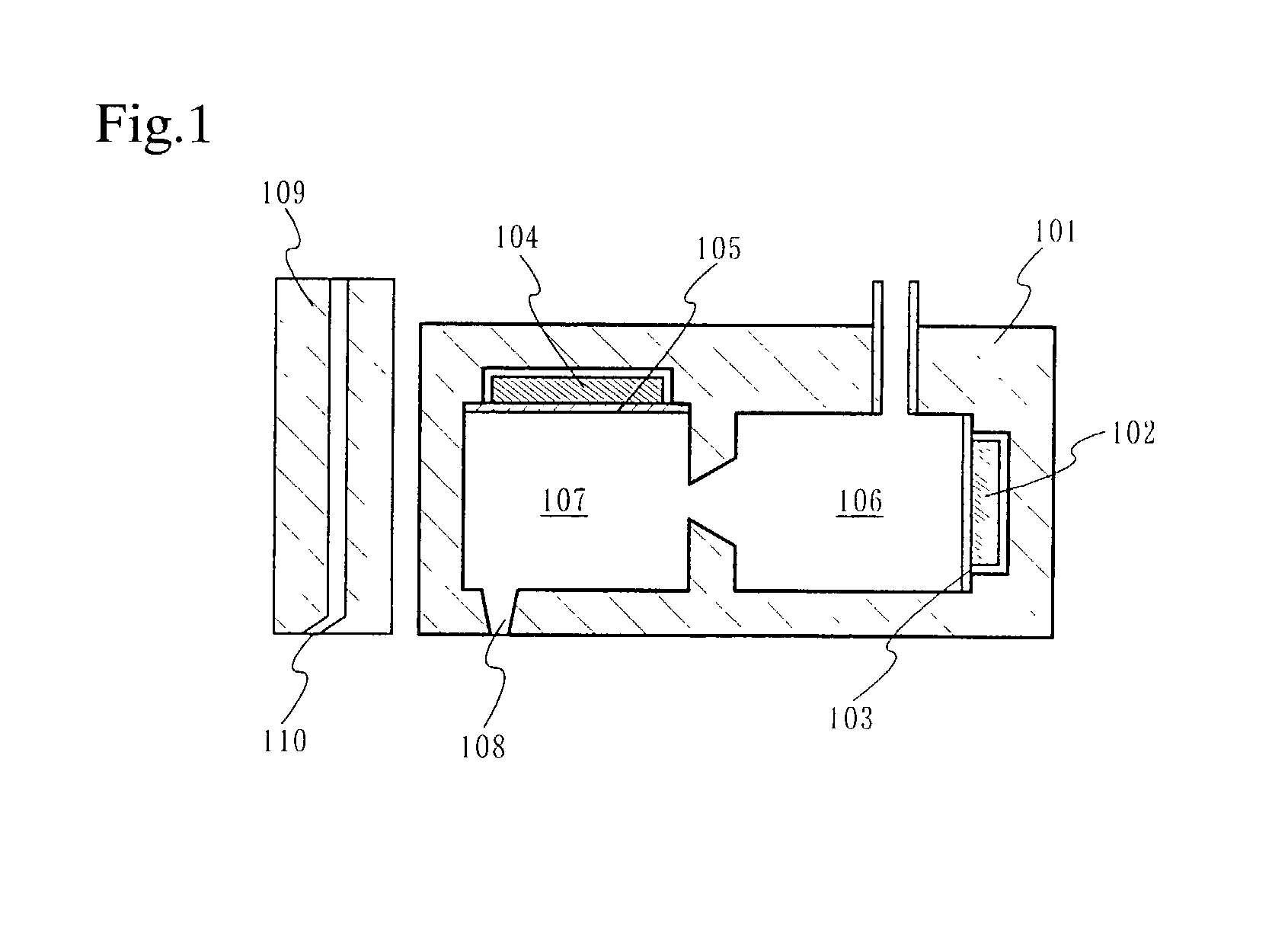
[0048]FIG. 6 schematically shows a state that a polymer organic compound layer is formed so as to match with a pixel region on a substrate in which one electrode of an organic light emitting clement by using an ink jet printing device according to the present invention. In FIG. 6, reference numeral 610 indicates a substrate, and a pixel region 611, a source side driver circuit 612 and a gate side driver circuit 613 are formed by using TFTs on the substrate 610. The pixel region corresponds to the region surrounded by a plurality of source wirings connected to the source side driver circuit 612 and a plurality of gate wirings connected to the gate side driver circuit 613. A TFT and an organic light emitting element electrically connected with the TFT are formed in the pixel region. The pixel region 611 is defined as the above-described region in which pixels are arranged in matrix.

[0049]Here, reference symbol 614a indicates a mixture of an organic compound material for emitting red l...

embodiment 2

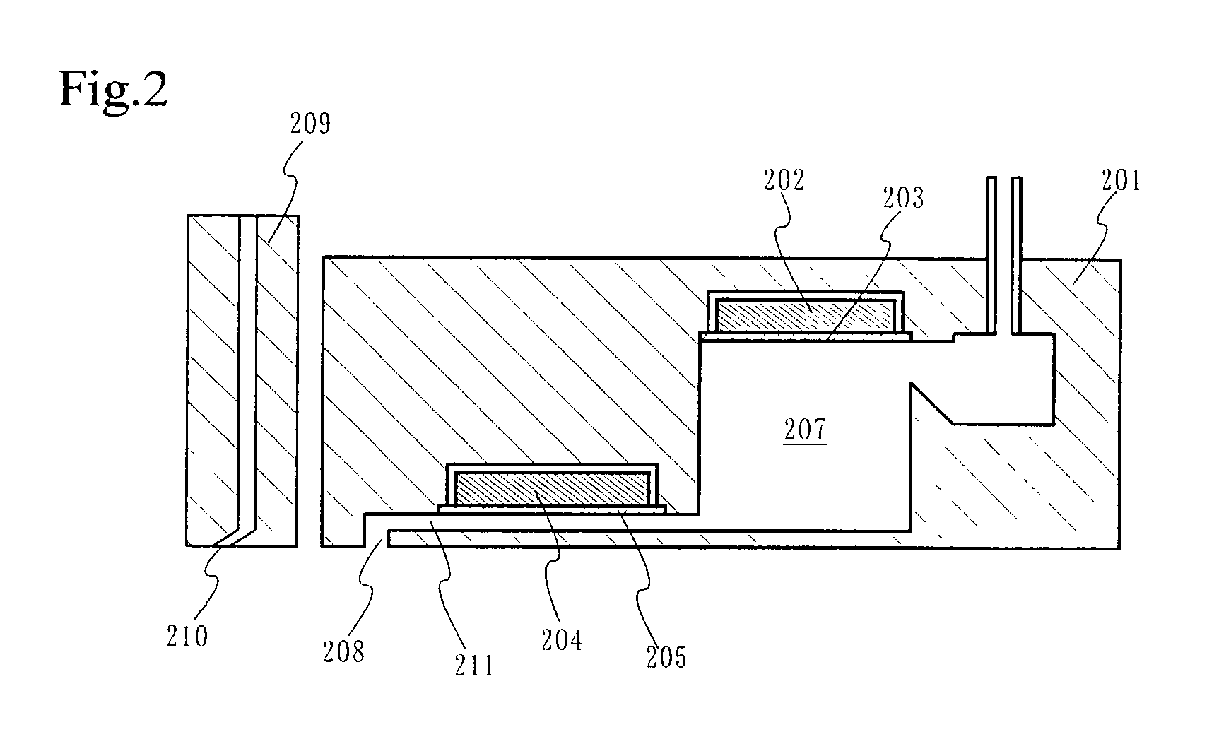
[0065]FIG. 7 schematically shows another example in which a polymer organic compound layer 614 is formed so as to correspond to a pixel region by using an ink jet printing device according to the present invention on a substrate on which one electrode of an organic light emitting element is formed. In FIG. 7, the same parts as those in FIG. 6 are indicated by the common reference numerals, and are not described here. FIG. 7 shows an embodiment in which application is conducted for each color, and one kind of the mixture is discharged from the ink head. In this case, the respective ink heads filled with the mixture for a red light emitting layer, the mixture for a green light emitting layer, and the mixture for a blue light emitting layer are provided, and application is conducted for each of the colors. Therefore, a thickness, a burning polymerization temperature in the later stage, and the like can be adjusted at the optimum level for each color.

embodiment 3

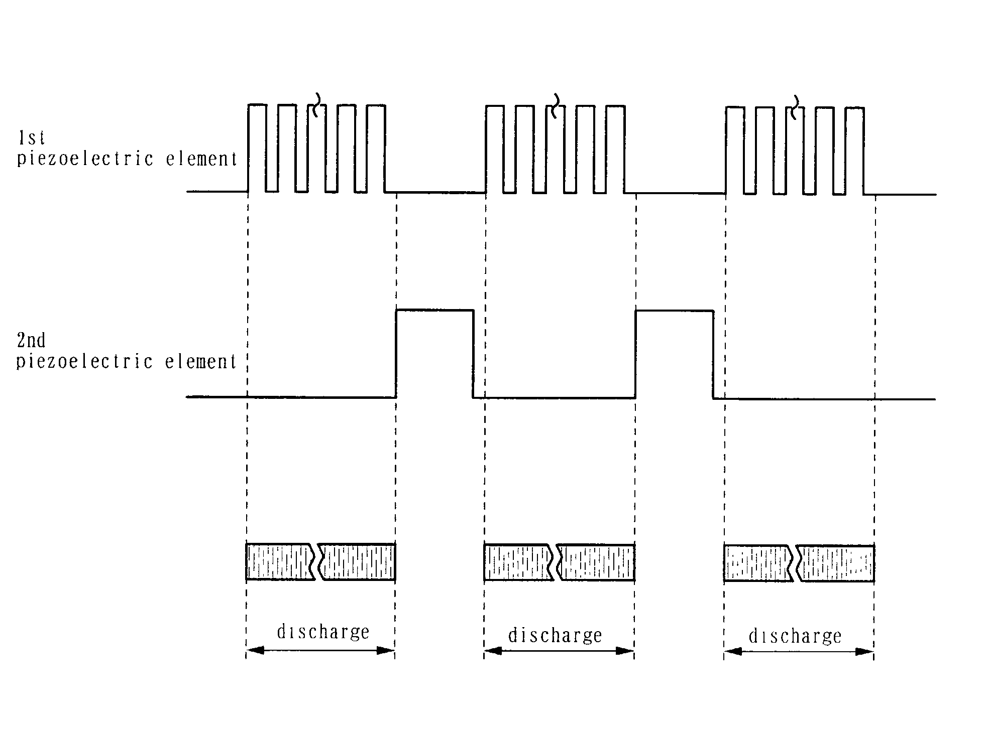
[0066]FIG. 8 shows an embodiment in which the printing device of the present invention is applied to a panel portion formed on a large-area substrate (mother glass substrate). On a mother glass substrate 800, panels 801a to 801f each including a pixel region with the same structure as that in FIG. 6 are formed. Although two ink heads 802a and 802b are shown in FIG. 8, the number of ink heads can be arbitrarily set. In the case where the mixture is applied continuously over the adjacent pixel regions, the first and second piezoelectric elements are incorporated into the ink head and the timings for causing displacement are synchronized, whereby the mixture can be discharged continuously or the discharge can be stopped instantaneously, as described using FIGS. 3A and 3B and FIG. 4. Accordingly, the organic compound layer can be formed at high speed with respect to the large-area substrate on which a large number of pixel regions are formed.


PUM

PropertyMeasurementUnit
depthaaaaaaaaaa
depthaaaaaaaaaa
sizeaaaaaaaaaa

Abstract

A first pressure generating chamber, which is sealed by a first elastic plate mounted with a first piezoelectric element at one surface, and a second pressure generating chamber, which is sealed by a second elastic plate mounted with a second piezoelectric element at one surface are formed in a casing. The second pressure generating chamber is formed with an opening which is a discharge port. A mixture is discharged from the discharge port. A nozzle formed with an opening jets gas toward a substrate surface, and is provided in the vicinity of the discharge port of the ink head.

Description

BACKGROUND OF THE INVENTION[0001]1. Field of the Invention[0002]The present invention relates to a method of manufacturing a light emitting device which has a light emitting element in which an emitter composed of an organic compound is provided between a pair of electrodes, and to a printing device which is applicable to the manufacture of the light emitting device.[0003]2. Description of the Related Art[0004]A light emitting element in which an organic compound is used for an emitter (hereinafter referred to as organic light emitting element) generally has a sandwich structure in which an organic compound layer is formed between a cathode and an anode. In case of using a low molecular weight organic compound, the structure is formed by combining layers such as a hole injecting layer, a hole transporting layer, a light emitting layer, an electron transporting layer and an electron injecting layer, which are composed of respective materials. The hole injecting layer and the hole tra...

Claims


Application Information

Patent Timeline
Patent Type & Authority Patents(United States)
IPC IPC(8): B05D5/06B05D5/12B41J2/01B05B17/06B05C5/00B05C5/02B05C11/04B05C11/06B05C11/10B05D1/26B41J2/005B41J2/045B41J2/055B41J2/14B41M3/00C09K11/06G09F9/00G09F9/30H01L21/77H01L21/84H01L27/12H01L27/32H01L51/00H01L51/30H01L51/40H01L51/50H01L51/56H05B33/04H05B33/10H05B33/12H05B33/22
CPCB05C11/1047B41J2/005B41M3/003H01L27/1214B05B17/0607H01L51/56B05C11/06B41J2202/11H01L51/0004H01L51/0005H01L51/0034H01L51/0035H01L51/0036H01L51/0037H01L51/0038B05C5/0275H01L29/78645H01L29/78648H01L27/1292H10K71/13H10K71/135H10K85/10H10K85/114H10K85/113H10K85/111H10K85/1135H10K71/40H10K71/00
Inventor YAMAZAKI, SHUNPEISEO, SATOSHI
Owner SEMICON ENERGY LAB CO LTD
Why Eureka
Try Eureka