Process for producing nitride semiconductor light-emitting device

a technology of nitride and semiconductor, which is applied in semiconductor devices, bulkheads/piles, foundation engineering, etc., can solve the problems of ni/au having only about 60% transmittance, large light loss due to absorption, and the inability of electrodes to mount on the back surface of the substrate,

Inactive Publication Date: 2006-06-20
SAMSUNG ELECTRONICS CO LTD
View PDF11 Cites 9 Cited by
  • Summary
  • Abstract
  • Description
  • Claims
  • Application Information

AI Technical Summary

Benefits of technology

[0015]Therefore, the present invention has been made in view of the above problems, and it is an object of the present invention to provide a process for producing a nitride semiconductor light-emitting device having an n-type nitride semiconductor layer arranged on a light-emitting side (generally, the side opposite the substrate) of an active layer by forming a p-type nitride semiconductor layer in such a manner that a heat treatment process to activate p-type impurities may be eliminated.
[0025]Preferably, the step of forming the n-type nitride semiconductor layer may comprise an additional forming of a high concentration n-type AlxInyGa1−(x+y)N (0≦x, y≦1) layer on the n-type nitride semiconductor layer. In this case, contact resistance with the n-electrode may be further improved.
[0031]The present invention provides a method for producing a structure having an n-type nitride semiconductor layer disposed on a light-emitting side relative to an active layer, and a p-type nitride semiconductor layer disposed between a substrate and the active layer. In this structure, the n-type nitride semiconductor layer having a low electrical resistance is disposed on the light-emitting side. Thus, there is an advantage of eliminating the step of forming a layer for improving contact resistance such as a transparent electrode layer or ITO layer.
[0032]Further, the present invention provides a solution to a problem involved in placement of the p-type nitride semiconductor layer between the substrate and active layer. That is, the conventional process requires a high temperature heat treatment or UV-annealing process in order to activate p-type impurities in the p-type nitride semiconductor layer. However, it presents not only problems of stopping a continuous nitride semiconductor growth and necessitating an additional heat treatment, but also damages crystal faces in which the active layer will grow, due to a heat treatment, resulting in an insurmountable problem, making it impossible to obtain high quality crystals. In order to overcome these disadvantages, the present invention provides a method of growing the p-type nitride semiconductor layer in which a subsequent heat treatment may be eliminated.

Problems solved by technology

These substrates for growth of nitride single crystals are electrically insulative, and thereby, electrodes cannot be mounted on the back surface of the substrate unlike conventional light-emitting devices.
However, the transparent electrode 18 made of Ni / Au has a transmissivity of only about 60%, suffering from great loss of light due to absorption.
Further, a complex process is required to add a layer for an ohmic contact of the above-mentioned transparent electrode layer.
A heat treatment process is needed to form NiO2 with a predetermined transmissivity after forming the Ni / Au layer, for instance, resulting in disadvantages of a complex process.
But, this method is not suitable for the p-type nitride semiconductor because of a heat treatment process required to activate p-type impurities.

Method used


Image

  • Process for producing nitride semiconductor light-emitting device
  • Process for producing nitride semiconductor light-emitting device
  • Process for producing nitride semiconductor light-emitting device

Examples


Embodiment Construction

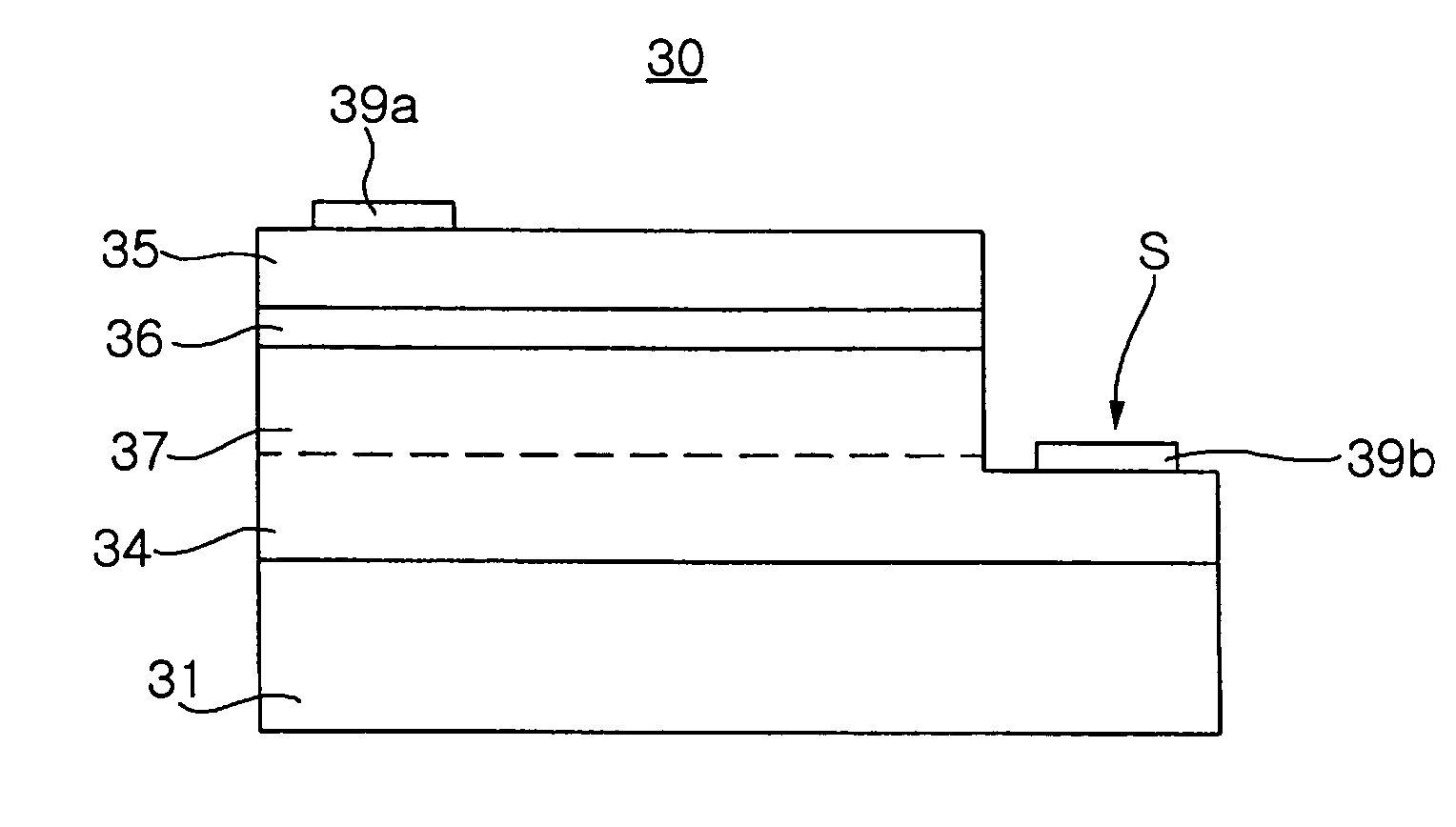
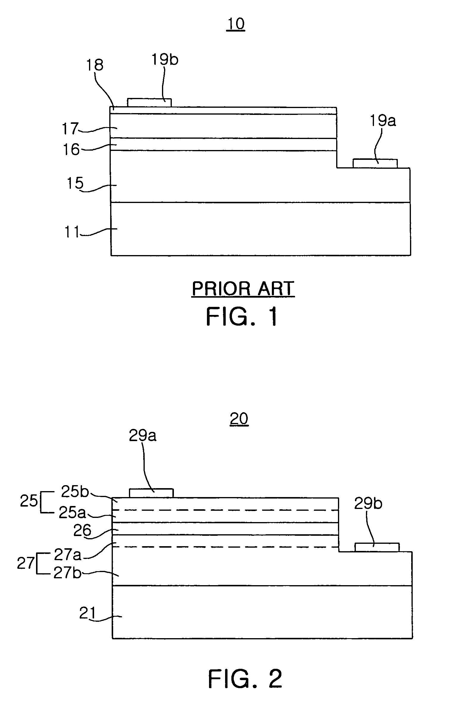
[0041]Preferred embodiments of the present invention will now be described in detail with reference to the annexed drawings. FIG. 2 is a cross-sectional side view of a nitride semiconductor light-emitting device 20 according to one embodiment of the present invention.

[0042]As shown in FIG. 2, the nitride semiconductor light-emitting device 20 includes a sapphire substrate 21, and a p-type nitride semiconductor layer 27, an active layer 26 and an n-type nitride semiconductor layer 25, these layers being formed sequentially on the sapphire substrate 21. Further, in order to improve a lattice matching of the p-type nitride semiconductor layer 27 with the sapphire substrate 21, a buffer layer may be formed thereon prior to growth of the p-type nitride semiconductor layer 27. As the buffer layer, a low temperature nucleus-growth layer made of a formula AlxInyGa1−(x+y)N (0≦x, y≦1) material may be used.

[0043]Referring now to FIG. 2, a process for producing the nitride semiconductor light-e...


PUM

PropertyMeasurementUnit
work functionaaaaaaaaaa
semiconductoraaaaaaaaaa
n-type conductiveaaaaaaaaaa

Abstract

A process for producing a nitride semiconductor light-emitting device includes the steps of preparing a substrate, growing a p-type nitride semiconductor layer on the substrate by the MOCVD process using hydrazine-based gas as a nitrogen precursor and N2 gas as a carrier gas, forming an active layer on the p-type nitride semiconductor layer, forming an n-type conductive nitride semiconductor layer on the active layer, and forming p- and n-electrodes in electrical connection with the p- and n-type nitride semiconductors, respectively.

Description

RELATED APPLICATIONS[0001]The present application is based on, and claims priority from, Republic of Korea Application Serial Number 2004-22115, filed Mar. 31, 2004, the disclosure of which is hereby incorporated by reference herein in its entirety.BACKGROUND OF THE INVENTION[0002]1. Field of the Invention[0003]The present invention relates to a process for producing a nitride semiconductor light-emitting device, and more particularly to a process for producing a nitride semiconductor light-emitting device having a novel structure in which a transparent electrode layer for improving contact resistance on a p-electrode may be eliminated.[0004]2. Description of the Related Art[0005]A nitride semiconductor light-emitting device is a high output power optical device that produces short wavelength light such as blue, green light, or the like, thus enabling it to produce a variety of colors, and attracts a great deal of attention in the related technical art[0006]A constituent material of...

Claims


Application Information

Patent Timeline
Patent Type & Authority Patents(United States)
IPC IPC(8): H01L21/00H01L21/20H01L21/205H01L21/28H01L21/3205H01L29/22H01L29/24H01L33/00
CPCH01L21/0237H01L21/0242H01L21/02458H01L33/007H01L21/02579H01L21/0262H01L21/0254E02D5/38E02D27/14E02D2250/0023E02D2300/0006E02D2600/20E02D2600/30
Inventor CHO, DONG HYUNKOIKE, MASAYOSHIHAHM, HUN JOO
Owner SAMSUNG ELECTRONICS CO LTD
Why Eureka
Try Eureka