Electron-emitting device, electron source and image-forming apparatus, and manufacturing methods thereof
an image-forming apparatus and electron-emitting technology, applied in the field of electron-emitting devices, electron-emitting apparatuses, and manufacturing methods thereof, can solve the problems of difficult to provide an image-forming apparatus with high luminance and excellent operating stability, and the stability of the electron-emitting characteristic and electron-emitting efficiency is not always satisfactory, so as to achieve a simple matrix arrangement
- Summary
- Abstract
- Description
- Claims
- Application Information
AI Technical Summary
Benefits of technology
Problems solved by technology
Method used
Image

Examples
example 1
(Example 1)
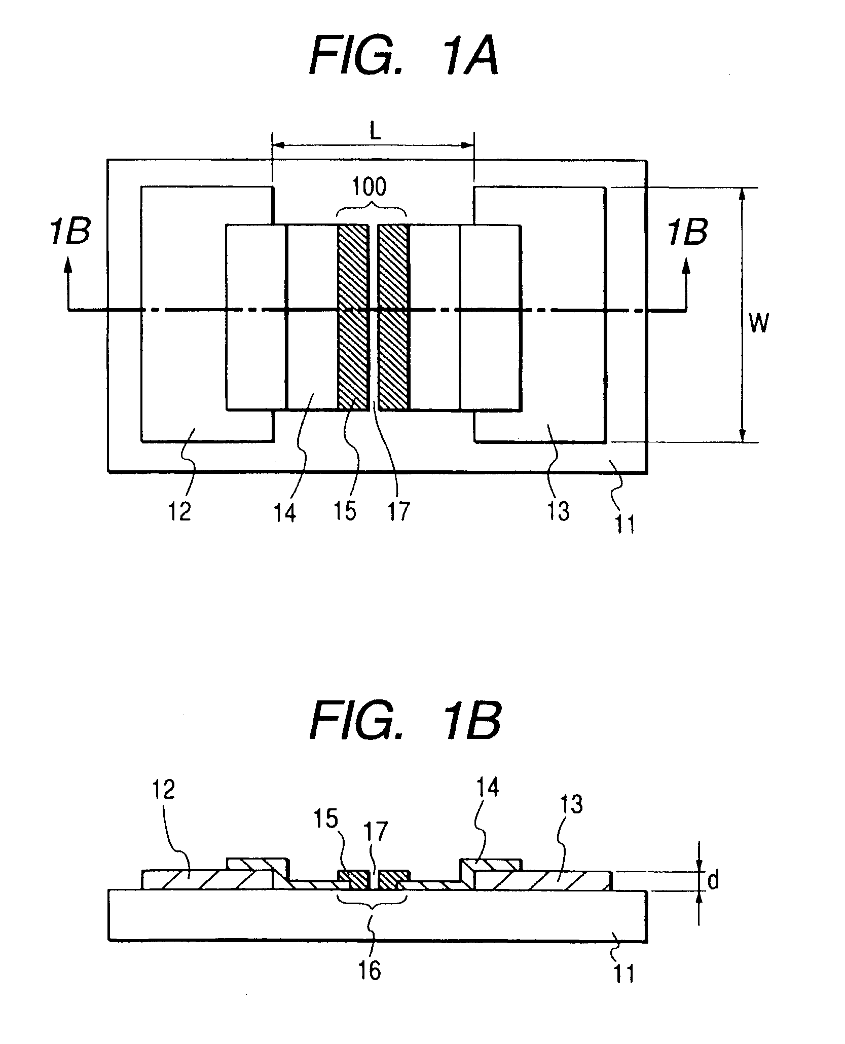
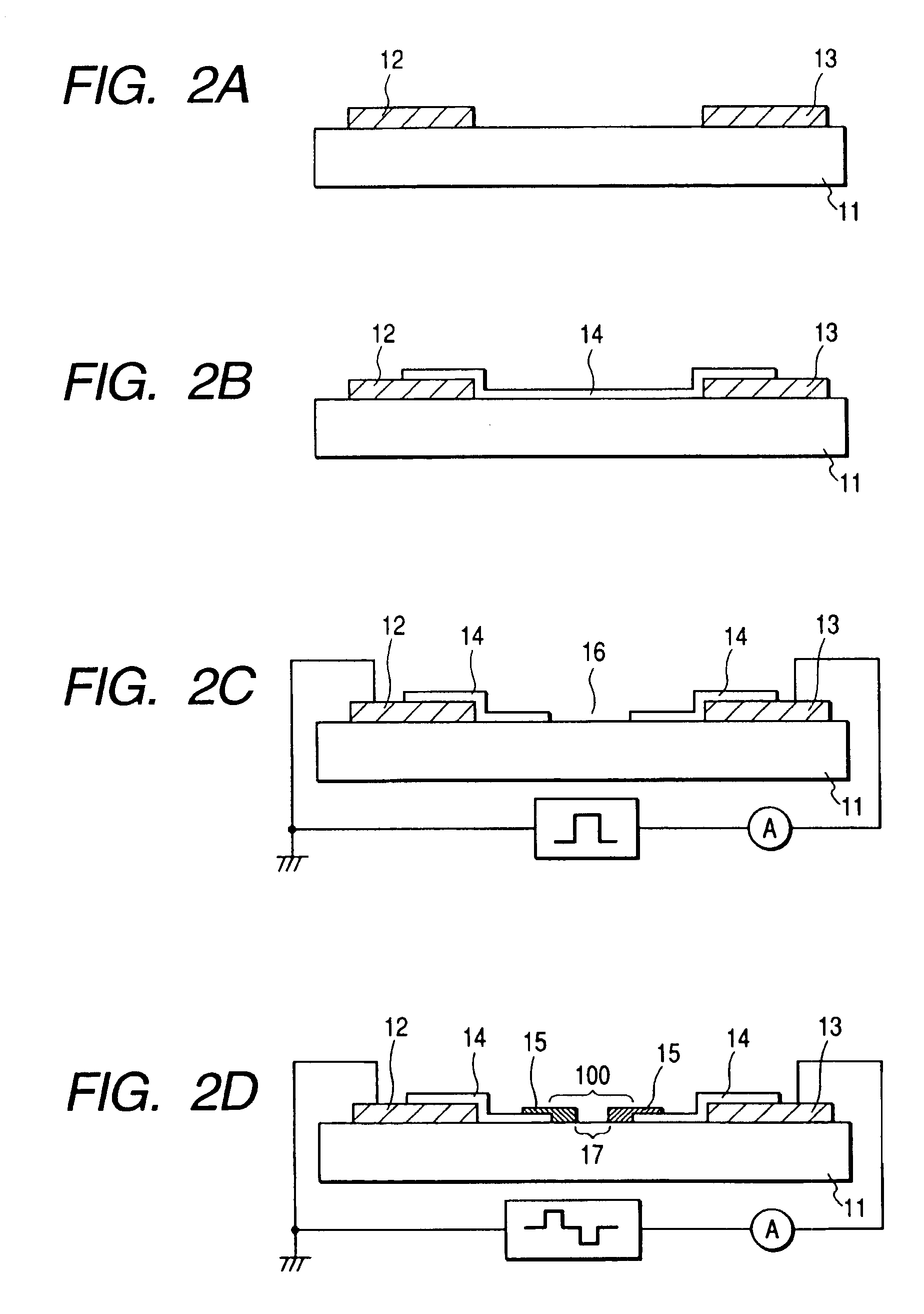
[0229]An electron-emitting device which has the configuration shown in FIGS. 1A and 1B was manufactured as Example 1 of the present invention. Example 1 will be described with reference to FIGS. 1A, 1B and 2A through 2D. Silica glass was used as the substrate 11, and Pt was used as a material of the device electrodes taking stability to humidity and stability to oxidation into consideration. Furthermore, thickness of the electrically conductive film 14 was set at 30 nm taking a resistance value between the device electrodes 12 and 13 into consideration. L was 20 μm, W was 100 μm and film thickness d was 10 nm in Example 1.
[0230]The electrically conductive film 14 was formed by coating the substrate 11 disposed the electrodes 12 and 13 with an organic Pd solution (“ccp-4230” prepared by Okuno Chemical Industries Co., Ltd.) to form an organometal film, heating the film for calcination and patterning the film (FIGS. 2A and 2B).
[0231]Then, a triangular wave pulse shown in FIG...
example 2
(Example 2)
[0239]As Example 2 of the present invention, an electron source which has the configuration shown in FIGS. 7A and 7B was manufactured through the activation step shown in FIGS. 9A and 9B.
[0240]In Example 2, basical configuration, materials and a manufacturing method were the same as those in Example 1, but L1, W and film thickness of an electrode was set at 5 μm, 100 μm and 10 nm respectively. Furthermore, width L2 of the common device electrode was set at 5 μm.
[0241]An electron-emitting device was formed through steps similar to those in Example 1 before formation of an electron emitting region. Then, the activation treatment was carried out by applying a pulse voltage in FIGS. 8A and 8B across the device electrodes 73 and 74 with the common device electrode set at a ground potential. In Example 2, acetone was introduced as an organic substance and kept at 1×10⁻⁵ Pa. The pulse width t1, the pulse voltage and the pulse interval t2 were set at 1 msec, 15 V and 200 msec res...
example 3
(Example 3)
[0246]In Example 3, an electron-emitting device having the configuration shown in FIGS. 21A and 21B was manufactured. Example 3 will be described with reference to FIGS. 21A, 21B, 22A, 22B and 23. Quartz was used as the substrate 11, and Pt was used as a material for the device electrodes 12 and 13 taking stability to humidity and stability to oxidation into consideration.
[0247]Then, the activation process was effected on the device.
[0248]Speaking concretely, a substrate on which the device electrodes 12 and 13 were formed was placed in the apparatus shown in FIG. 23, acetone was introduced as an organic substance gas into vacuum sufficiently evacuated with an ion pump or the like and maintained at 1×10⁻⁵ Pa, and pulses shown in FIG. 8A were applied across the electrodes 12 and 13. T1 and t2 shown in FIG. 8A were set at 1 msec and 10 msec respectively. Simultaneously, the substrate was irradiated with an electron beam with an accelerating voltage set at 2 kV.
[0249]Forming...
PUM
 Abstract
Description
Claims
Application Information