Optical scanning device for reducing a dot position displacement at a joint of scanning lines
a scanning device and scanning line technology, applied in the direction of mountings, instruments, printing, etc., can solve the problems of increasing power consumption, deteriorating image quality, and inconvenience of different heights of scanning lines formed on scanned surfaces
- Summary
- Abstract
- Description
- Claims
- Application Information
AI Technical Summary
Benefits of technology
Problems solved by technology
Method used
Image

Examples
first embodiment
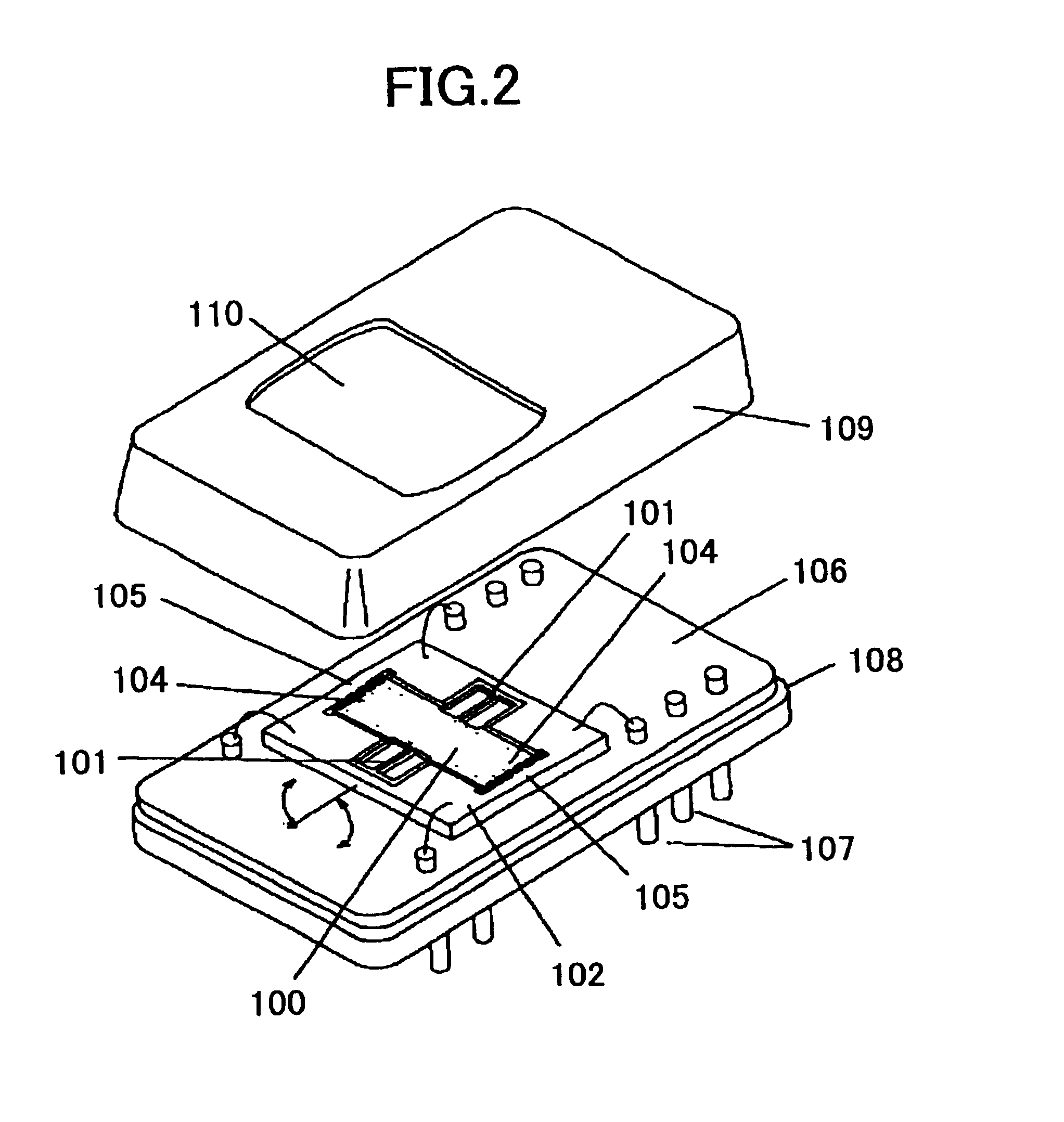
[0104]FIG. 2 illustrates an oscillation mirror deflector used in an optical scanning device according to the present invention. In FIG. 2, a mirror substrate is formed by etching a silicon substrate 102 so as to form a quadrilateral opening in a back surface thereof and to leave a frame portion and a top plate portion with a predetermined thickness. The top plate portion is formed by leaving an oscillation mirror 100 and torsion bars 101 as an axle bearing the oscillation mirror 100, and by penetrating the perimeter of the oscillation mirror 100 and the torsion bars 101. In the present embodiment, using a silicon substrate having a thickness of 200 μm, the oscillation mirror 100, i.e., the top plate portion, is formed 60 μm thick. The oscillation mirror 100 has a size of 4 mm×2 mm. The oscillation mirror 100 has an upper surface formed as a reflective surface by depositing a coating of metal, such as Cu (copper). The oscillation mirror 100 has projecting and receding parts in pectin...
second embodiment
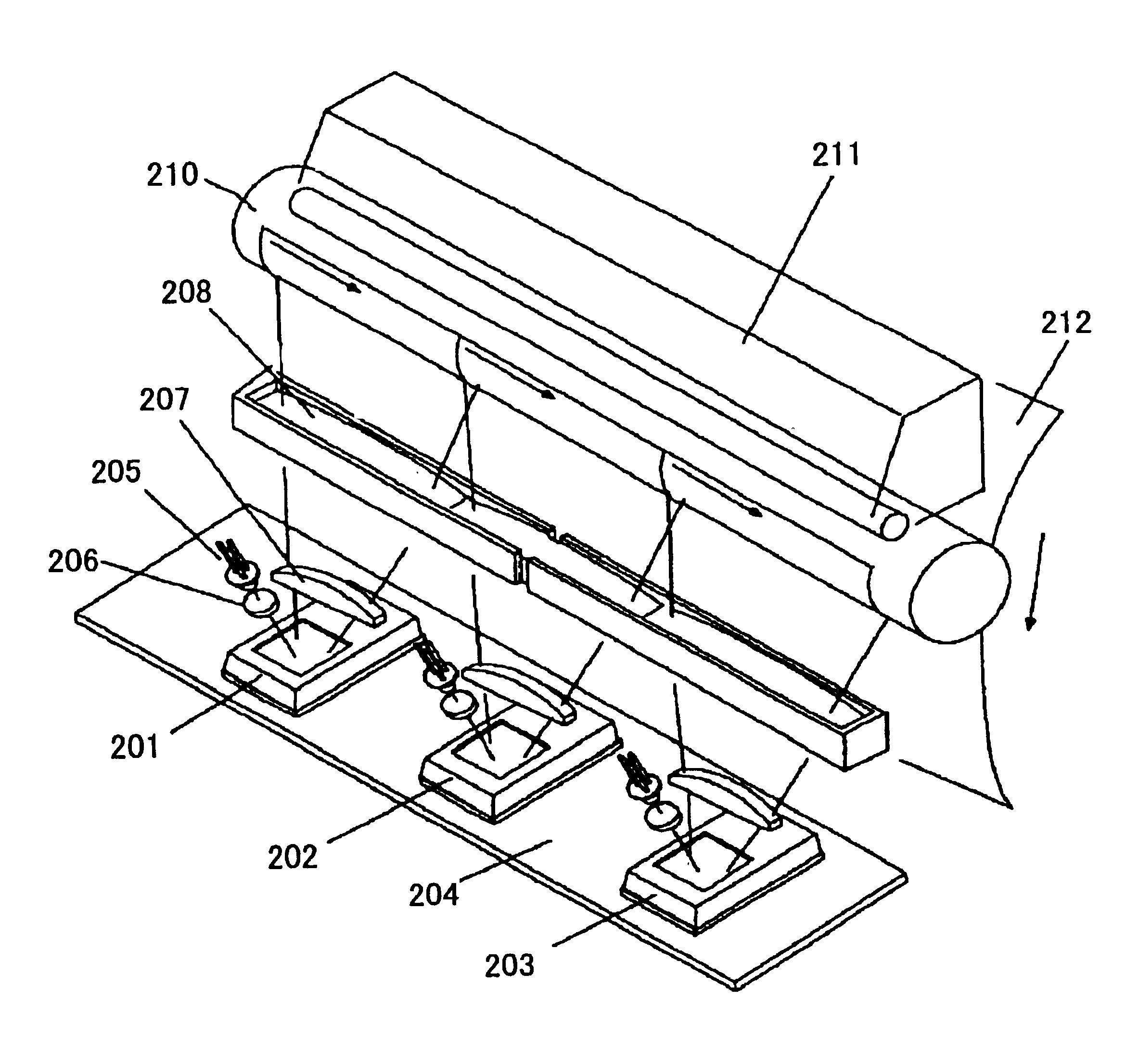
[0115]FIG. 4 illustrates an optical scanning device according to the present invention. In FIG. 4, four oscillation mirror deflectors 220, 221, 222 and 223 are arranged in parallel in a sub-scanning direction on an electrical substrate (not shown in the figure in the present embodiment). The oscillation mirror deflectors 220, 221, 222 and 223 are deflecting units each of which performs an optical scanning by oscillation. The oscillation mirror deflectors 220, 221, 222 and 223 are combined with respective semiconductor lasers 225, respective coupling lenses 226, respective first scanning lenses 227, and respective second scanning lenses 228 so as to form respective scanning optical systems. The scanning optical systems record electrostatic latent images corresponding to yellow (Y), magenta (M), cyan (C) and black (K), respectively, on image bearers 230, 231, 232 and 233, each of which is formed by a photosensitive drum and so forth, arranged along a feeding direction of a transfer be...
third embodiment
[0126]In the above-described embodiment, the timing of the image recording is changed in a same manner every predetermined number of scanning periods; however, the timing of the image recording may be changed in a different manner every predetermined number of scanning periods. FIG. 8 illustrates how a displacement of scanning lines is corrected according to the present invention. To make the description simple, only two scanning optical systems are arranged also in the following example. In FIG. 8, a transverse direction is the main scanning direction, and a vertical direction is the sub-scanning direction. An image recording is performed only in the “forth” period of the reciprocating oscillation. As described above, when the scanning optical systems are driven by individual scanning frequencies, the scanning lines come close to one another in the vertical direction, since a scanning frequency with respect to the scanning lines at the right is higher than a scanning frequency with...
PUM
 Abstract
Description
Claims
Application Information
 - Generate Ideas
- Intellectual Property
- Life Sciences
- Materials
- Tech Scout
- Unparalleled Data Quality
- Higher Quality Content
- 60% Fewer Hallucinations
Browse by: Latest US Patents, China's latest patents, Technical Efficacy Thesaurus, Application Domain, Technology Topic, Popular Technical Reports.
© 2025 PatSnap. All rights reserved.Legal|Privacy policy|Modern Slavery Act Transparency Statement|Sitemap|About US| Contact US: help@patsnap.com