

Charge pump circuit
a pump circuit and pump technology, applied in pulse generators, pulse techniques, instruments, etc., can solve the problems of bringing about the danger of other vehicle-mounted apparatuses of radio or the like, the drawback of bringing about an increase in cost or a dimension and a weight, and achieve the effect of considerable noise and short period of tim
- Summary
- Abstract
- Description
- Claims
- Application Information
AI Technical Summary
Benefits of technology
Problems solved by technology
Method used
Image

Examples
first embodiment
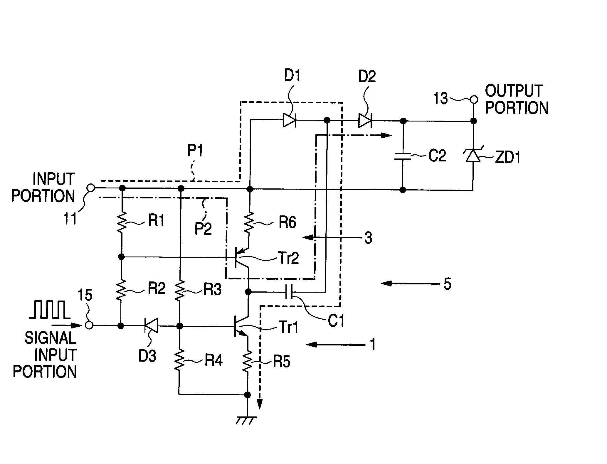
[0018]FIG. 1 is a circuit diagram of a charge pump circuit according to the invention. As shown by FIG. 1, the charge pump circuit is constituted by including a first through a third diode D1 through D3, first and second capacitors C1, C2, first and second transistors Tr1, Tr2, first through sixth resistors R1 through R6, a Zener diode ZD1, and a driving circuit (driver), not illustrated, for driving the transistors Tr1, Tr2. Among them, the capacitor C1 corresponds to a stepping up capacitor according to the invention. Further, a combination of the transistor Tr1 and the resistor R5 and a combination of the transistor Tr2 and the resistor R6 respectively constitute follower circuits 1, 3 according to the invention and the follower circuits 1, 3, the resistors R1 through R3 and the diode D3 constitute a constant current charging and discharging circuit 5. Further, the transistors Tr1, Tr2 serve also as first and second switches according to the invention. Further, a bipolar type NPN...
second embodiment
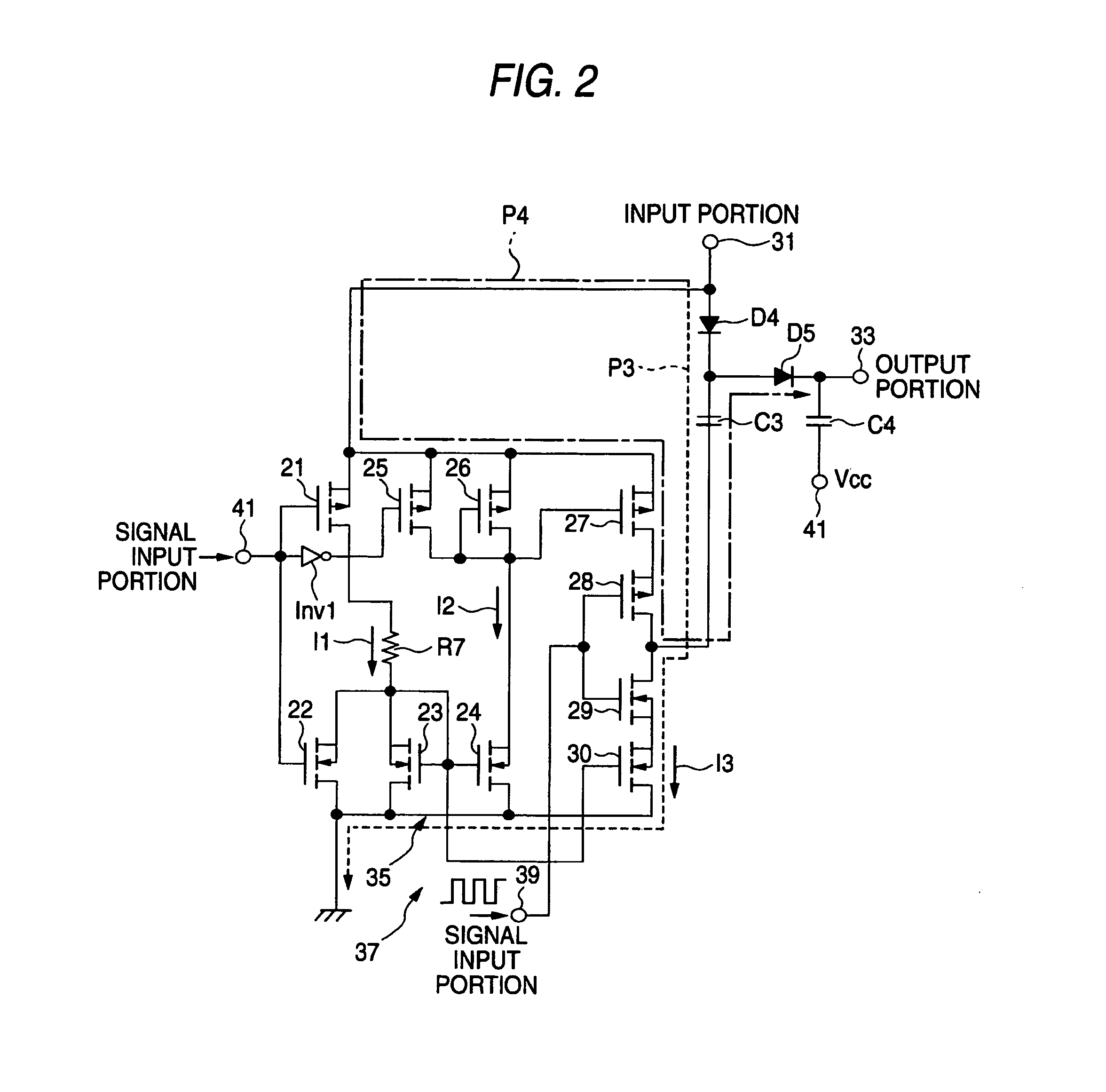
[0034]FIG. 2 is a circuit diagram of a charge pump circuit according to the invention. As shown by FIG. 2, the charge pump circuit is constituted by including first and second diodes D4, D5, first and second capacitors C3, C4, first thought tenth FETs 21 through 30, a resistor R7, an inverter Inv1, and a driving circuit (driver), not illustrated, for driving FETs 28, 29. Among them, the capacitor C3 corresponds to a capacitor for stepping up according to the invention, FET 29 corresponds to a first switch according to the invention, and FET 28 corresponds to a second switch according to the invention. Further, FETs 23, 24, 30 constitute a current mirror circuit (MOSFET Weidler current mirror circuit) 35, and FETs 23, 24, 27 including FETs 23, 24, 30 constitute a constant current charging and discharging circuit 37. Here, FETs 21, 25 through 28 are P-channel MOSFETs and FETs 22 through 24, 29, 30 are N-channel MOSFETs.
[0035]Further, the charge pump circuit according to the second emb...
PUM
 Abstract
Description
Claims
Application Information