Bus control device altering drive capability according to condition

a technology of drive capability and control device, which is applied in the direction of logic circuit coupling/interface arrangement, pulse technique, instruments, etc., can solve the problems of etc., to prevent unnecessary power consumption and noise generation

Inactive Publication Date: 2006-07-18
RENESAS ELECTRONICS CORP
View PDF9 Cites 0 Cited by
  • Summary
  • Abstract
  • Description
  • Claims
  • Application Information

AI Technical Summary

Benefits of technology

[0010]It is an object of the present invention to provide a bus control device capable of preventing unnecessary power consumption and generation of noise by altering a drive capability of a bus according to a region to which an access is made by a CPU or the like.
[0011]It is another object of the present invention to provide a bus control device capable of preventing unnecessary power consumption and generation of noise by altering a drive capability of a bus according to the number of bus waits.
[0012]It is still another object of the present invention to provide a bus control device capable of preventing unnecessary power consumption and generation of noise by altering a drive capability of a bus according to a bus operating frequency.
[0014]Since the logic circuit controls the plurality of output buffers according to a region at an access destination and a drive capability of a bus corresponding thereto, the drive capability of a bus can be altered according to a region to which an access is made by a CPU or the like, thereby enabling prevention of unnecessary power consumption and generation of noise.
[0016]Since the logic circuit controls the plurality of output buffers by comparing the number of bus waits and a threshold value of the number of bus waits with each other, a drive capability of a bus can be altered according to the number of bus waits, thereby enabling prevention of unnecessary power consumption and generation of noise.
[0018]Since the logic circuit controls the plurality of output buffers by comparing a bus operating frequency and a threshold value of a bus operating frequency with each other, a drive capability of a bus can be altered according to the bus operating frequency, thereby enabling prevention of unnecessary power consumption and generation of noise.

Problems solved by technology

Of semiconductor devices connected to the same external bus, however, such a drive capability is in excess of requirement to a device with characteristics of larger required values for a delay time, and rise and fall times of a bus signal and the bus is driven to an excessive level when an access is made to the device, having resulted in a problem causing unnecessary power consumption and generation of noise.
Furthermore, in a case where a frequency of an operating clock for a CPU or the like is lowered in order to operate an external bus in a low power consumption mode as well, a bus is driven to an excessive level, also having led to a problem causing unnecessary power consumption and generation of noise.

Method used


Image

  • Bus control device altering drive capability according to condition
  • Bus control device altering drive capability according to condition
  • Bus control device altering drive capability according to condition

Examples


first embodiment

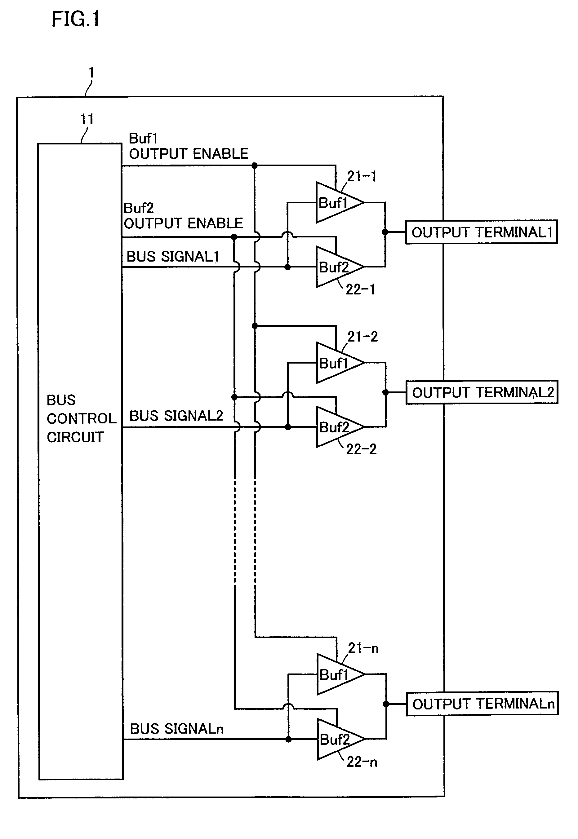
[0025]FIG. 1 is a block diagram showing a schematic configuration of a semiconductor device on which a bus control device is mounted in a first embodiment of the present invention. A semiconductor device 1 includes: a bus control circuit 11; buffers 1 (hereinafter referred to as Buf1) 21-1 to 21-n connected to respective output terminals 1 to n; and buffers 2 (hereinafter referred to as Buf2) 22-1 to 22-n connected to respective output terminals 1 to n. Note that Buf1s (21-1 to 21-n) and Buf2s (22-1 to 22-n), both provided correspondingly to respective output terminals 1 to n, are each referred to as an output buffer section. In addition, bus control circuit 11 and output buffer sections are collectively referred to as a bus control device. Buf1s (21-1 to 21-n) and Buf2s (22-1 to 22-n) may have either the same drive capability as, or drive capabilities different from each other.

[0026]A Buf1 output enable signal output from bus control circuit 11 is connected to output enable termina...

second embodiment

[0042]A schematic configuration of a semiconductor device on which a bus control device is mounted in a second embodiment of the present invention is similar to the schematic configuration of the semiconductor device on which the bus control device is mounted in the first embodiment shown in FIG. 1. Therefore, no detailed description of duplicated parts of the configuration and functions thereof will be repeated.

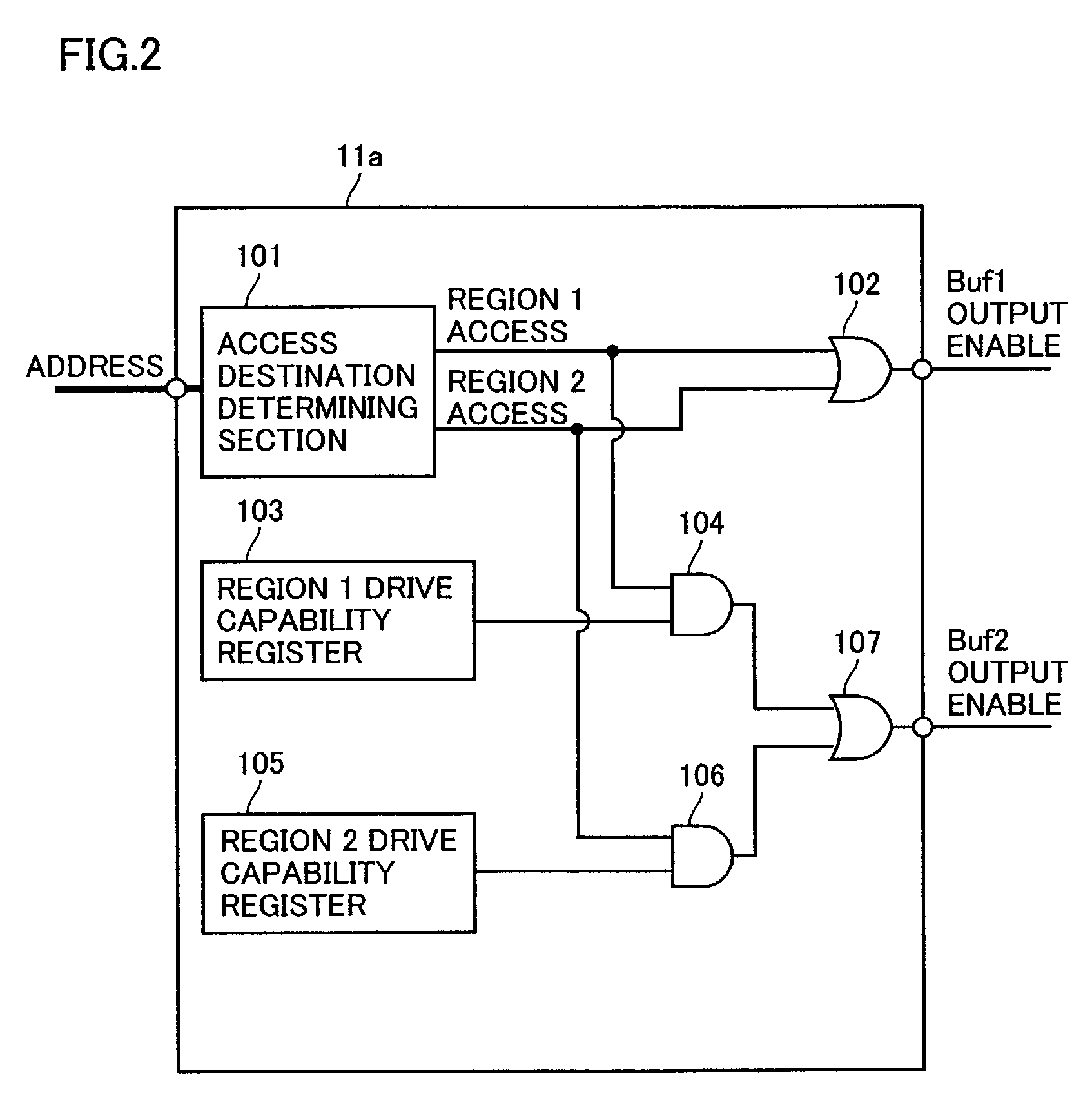
[0043]FIG. 3 is a block diagram showing a configuration of a bus control circuit 11b in the second embodiment of the present invention. Bus control circuit 11b includes: an access destination determining section 101 decoding an address output from the CPU which is not shown or the like to determine an address destination; a region 1 wait threshold value register 201 in which there is set a threshold value of the number of waits when an access is made to region 1 determined by access destination determining section 101; a region 1 number-of-waits register 202 in which there i...

third embodiment

[0060]A schematic configuration of a semiconductor device on which a bus control device is mounted in a third embodiment of the present invention is similar to the schematic configuration of the semiconductor device on which the bus control device is mounted in the first embodiment shown in FIG. 1. Therefore, no detailed description of duplicated parts of the configuration and functions thereof will be repeated.

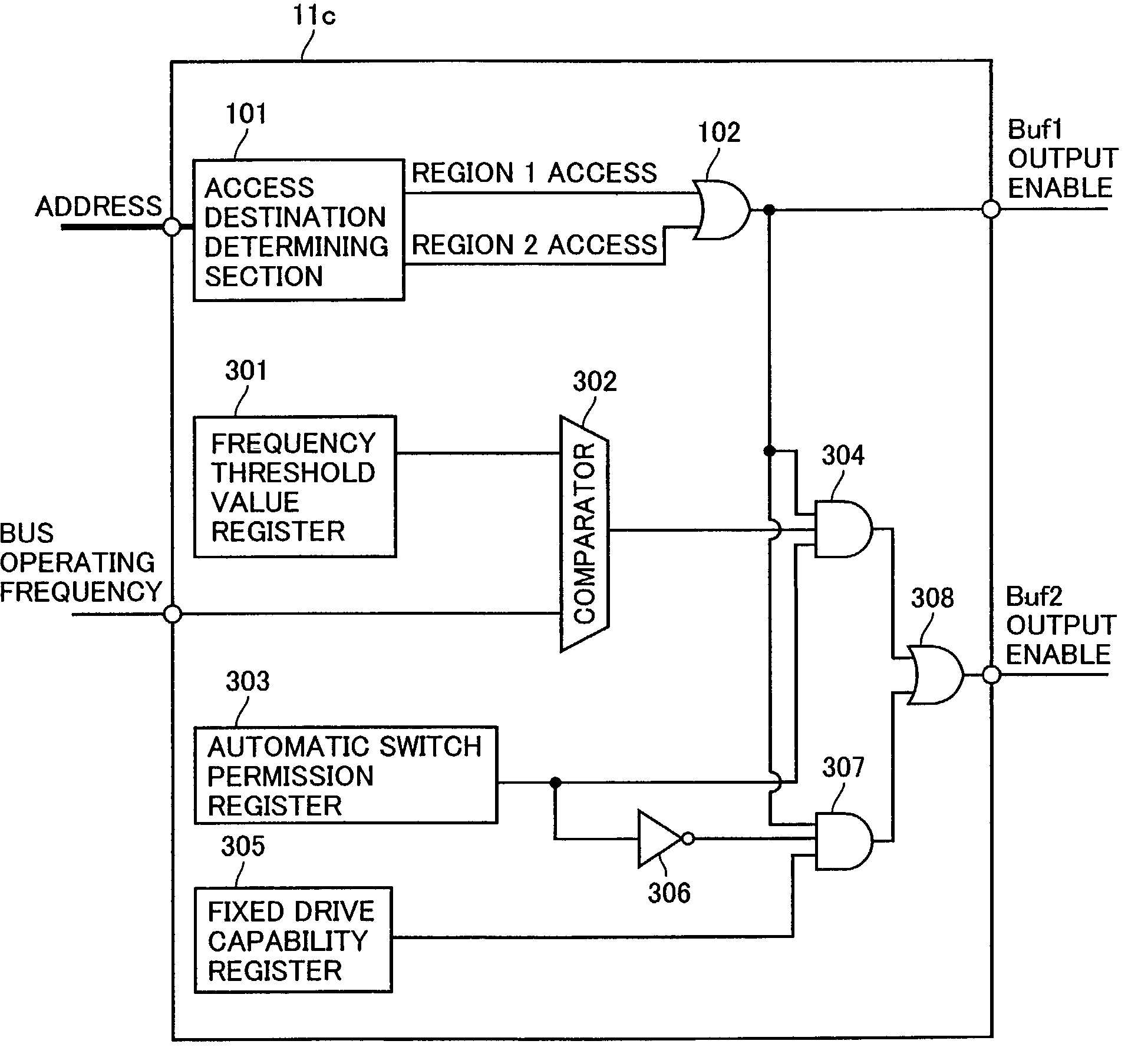
[0061]FIG. 4 is a block diagram showing a configuration of a bus control circuit 11c in the third embodiment of the present invention. Bus control device 11c includes: an access destination determining section 101 decoding an address output from the CPU which is not shown or the like to determine an access destination; a frequency threshold value register 301 in which a threshold value of a bus operating frequency is set; an automatic switch permission register 303 in which setting is effected of information on whether or not automatic switching between drive capabilities of ...


PUM


Abstract

An access destination determining section determines whether an access is directed to region 1 or region 2. A region 1 drive capability register and a region 2 drive capability register set drive capabilities of output buffers when accesses to region 1 and region 2 generate, respectively. For example, if “1” is set to region 1 drive capability register, when an access to region 1 generates, a Buf2 output enable signal is output at high level to enable outputs of Buf2s. Therefore, a drive capability of a bus can be altered according to a region to which an access is made by a CPU or the like, thereby enabling prevention of unnecessary power consumption and generation of noise.

Description

BACKGROUND OF THE INVENTION[0001]1. Field of the Invention[0002]The present invention relates to a technique controlling a drive capability of a bus such as a data bus or an address bus, and more particularly to a bus control device capable of altering a drive capability of a bus according to a region to which an access is made by a CPU (Central Processing Unit) or the like, an operating condition for the bus or the like.[0003]2. Description of the Background Art[0004]In recent years, a system on which a CPU is mounted has been progressed in its high functionality and multi-functionality and along this progress, various semiconductor devices have been connected to a bus in the system. Since kinds and the number of semiconductor devices connected to a bus are different according to a system and, in addition, a load capacity of a bus varies according to a system, a drive capability of an output buffer for a semiconductor device is demanded in various ways.[0005]In such circumstances, ...

Claims


Application Information

Patent Timeline
Patent Type & Authority Patents(United States)
IPC IPC(8): G06F13/14H01L25/00H03F3/00H03K19/0175G06F3/00G06F1/32G06F13/00G06F13/36
CPCG06F1/3203G06F1/3253Y02B60/1235Y02D10/00
Inventor KURAFUJI, TAKASHI
Owner RENESAS ELECTRONICS CORP
Why Eureka
Try Eureka