Method of producing plasma display devices
- Summary
- Abstract
- Description
- Claims
- Application Information
AI Technical Summary
Benefits of technology
Problems solved by technology
Method used
Image
Examples
Embodiment Construction
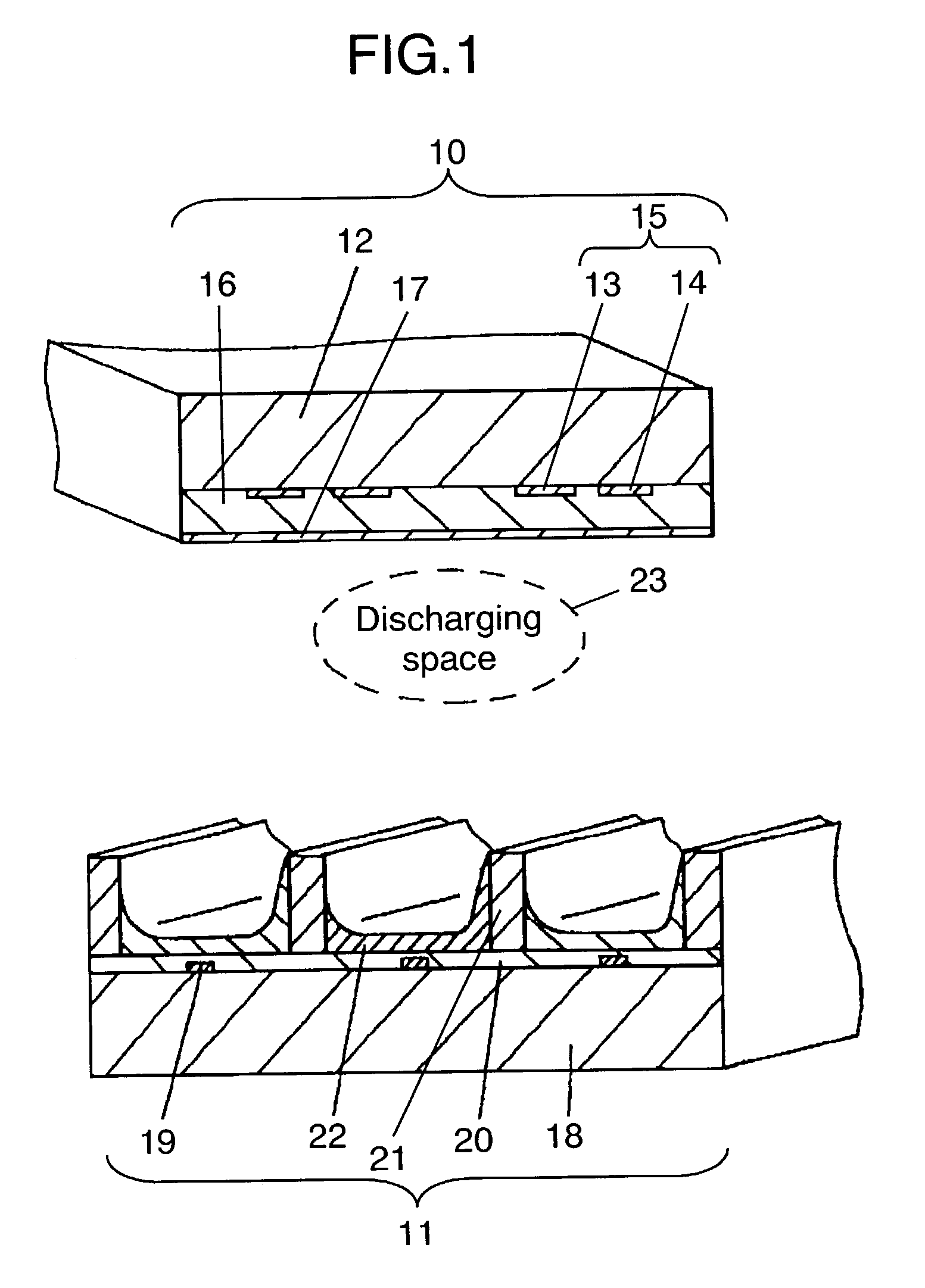
[0026]An exemplary embodiment of the present invention is described hereinafter with reference to FIGS. 1 to 7.
[0027]FIG. 1 is a perspective sectional view showing a panel structure of a plasma display apparatus. The panel is formed of front panel portion 10 and rear panel portion 11. Front panel portion 10 is formed of front substrate 12, display electrode 15, dielectric layer 16 and protective film 17. Front substrate 12 is made of transparent substrate such as glass. Display electrodes 15 are formed of a plurality of scanning electrodes 13 and a plurality of sustain electrodes 14, which are formed on front substrate 12, where scanning electrode 13 and sustain electrode 14 form a pair and striped pattern. Dielectric layer 16 is formed on front substrate 12 with display electrodes 15 covered. Protective film 17 is formed on dielectric layer 16.
[0028]Rear panel portion 11 opposing to front panel 10 is formed of rear substrate 18, address electrode 19, overcoat layer 20, barrier rib ...
PUM
 Abstract
Description
Claims
Application Information


