Horizontal TRAM and method for the fabrication thereof

a technology of horizontal trams and sram cells, which is applied in the direction of sram devices, basic electric elements, electrical apparatus, etc., can solve the problems of inhibiting the use of commercial sram products, limiting the maximum density of such srams, and conventional ndr-based sram cells, so as to reduce the number of implantation steps, avoid additional complexity and expense in fabrication and manufacturing processes, and avoid contact-formation problems

Active Publication Date: 2006-07-25
CHARTERED SEMICONDUCTOR MANUFACTURING
View PDF10 Cites 47 Cited by
  • Summary
  • Abstract
  • Description
  • Claims
  • Application Information

AI Technical Summary

Benefits of technology

[0026]The present invention provides a method for manufacturing an integrated circuit structure. A semiconductor substrate is provided and a trench is formed therein. A thyristor is formed around the trench and within the semiconductor substrate, the thyristor having at least four layers with three P-N junctions therebetween. A gate for the thyristor is formed within the trench. An access transistor is formed on the semiconductor substrate; and an interconnect is formed between the thyristor and the access transistor. Thus, there is provided a thyristor-based SRAM and advanced methods for the fabrication thereof that alleviate the contact-formation problems due to the large height difference among contacts in the cell, that reduce the number of implantation steps, that do not require epitaxial formation procedures, and that allow salicidation. Further, the advanced device structures and methods use existing bulk processing techniques, thereby avoiding additional complexity and expense in the fabrication and manufacturing processes so as to be highly manufacturable, reliable, scalable, repeatable and economical to produce.

Problems solved by technology

SRAM and DRAM often compromise one or more of the primary design goals of smaller circuit space, lower power consumption, and faster circuit speed.
However, the 4T and 6T cells are conventionally configured using a large cell area; and this large area significantly and undesirably limits the maximum density of such SRAMs.
Conventional NDR-based SRAM cells, however, have many problems that have inhibited their use in commercial SRAM products.
Some of these problems include: high standby power consumption due to the large current needed in one or both of the stable memory states of the cell; excessively high or excessively low voltage levels needed for the cell operation; stable states that are too sensitive to manufacturing variations and provide poor noise-margins; limitations in access speed due to slow switching from one stable state to the other; and manufacturability and yield issues due to complicated fabrication processing.
For use in electronic applications, however, a significant difficulty with thyristor devices is that once switched to their on state, they remain in this state until the current is reduced below the device holding current.
This inability to switch the device off without interrupting the current, and the associated slow switching speed, are significant problems in many applications and have resulted in many attempts to modify the device structures so that they can be actively and rapidly switched off.
However, the TRAM cell disclosed in these patents presents several major drawbacks.
This is not compatible with conventional bulk CMOS processing.
This results in a large difference in elevation between the contact on the top P+ region of the thyristor and other contacts in the device.
There is also potential incompatibility with salicidation.
Additionally, difficulties can arise in controlling the dimensions of the vertical pillar and reproducing these dimensions for each TRAM cell in a TRAM array.
Also, due to the existence of a vertical thyristor in each TRAM cell, the TRAM cells as a whole are not planar and are therefore difficult to scale to larger configurations.
Additionally, since each TRAM cell is fabricated prior to or after fabricating other devices (such as positive-channel metal-oxide semiconductor (“PMOS”) and negative-channel metal-oxide semiconductor (“NMOS”) supporting devices) that are connected to it, extra fabrication steps and increased manufacturing costs are incurred.
Thus, while there is a growing trend to realize an SRAM cell by using the TRAM combination of an NPNP junction connected to an NMOS transistor for ultra-high cell density, the incompatibility with conventional bulk CMOS processing makes such embedded SRAM design difficult.
Solutions to problems of this sort have been long sought, but have long eluded those skilled in the art.

Method used


Image

  • Horizontal TRAM and method for the fabrication thereof
  • Horizontal TRAM and method for the fabrication thereof
  • Horizontal TRAM and method for the fabrication thereof

Examples


Embodiment Construction

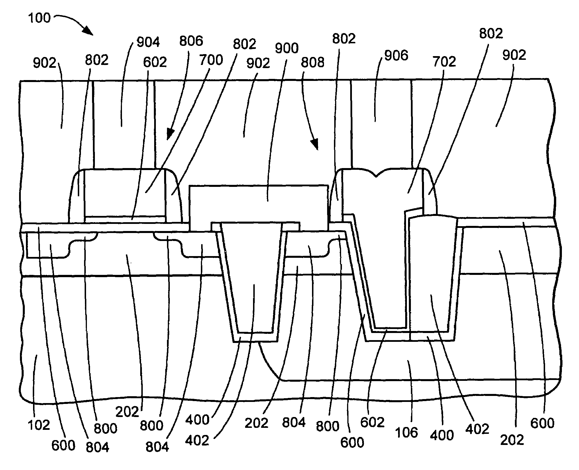
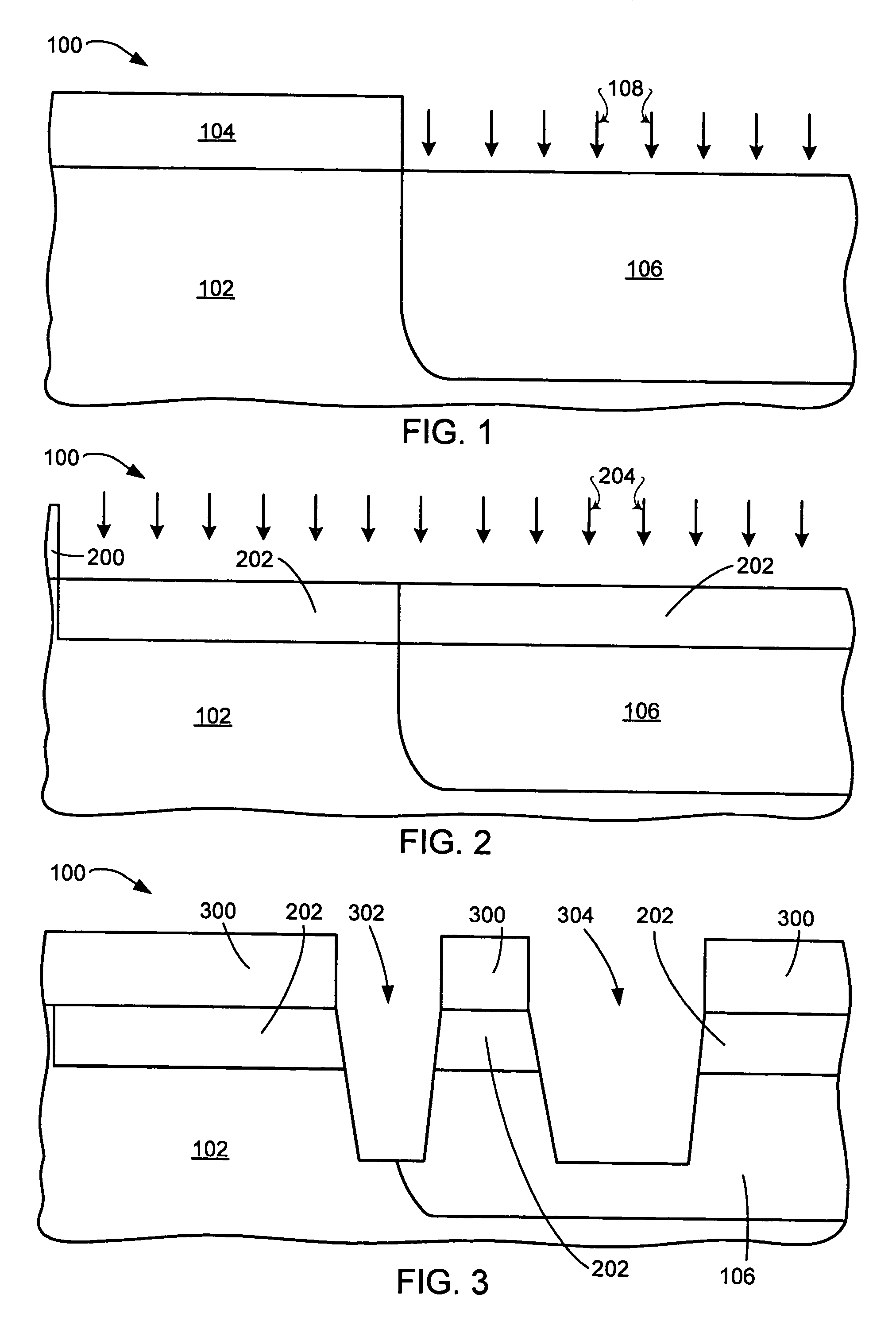
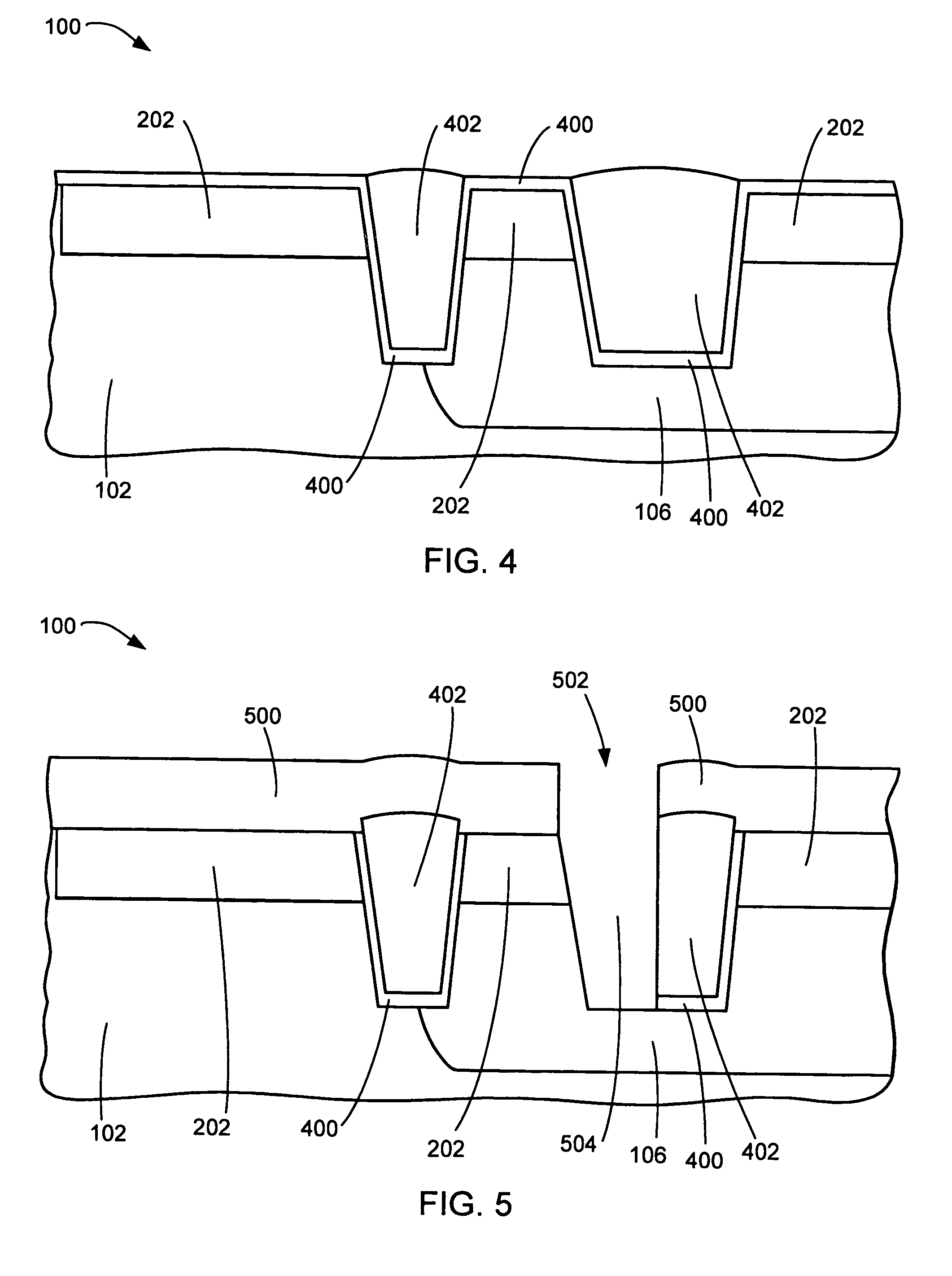
[0038]In the following description, numerous specific details are given to provide a thorough understanding of the invention. However, it will be apparent to one skilled in the art that the invention may be practiced without these specific details. In order to avoid obscuring the present invention, some well-known configurations and process steps are not disclosed in detail. Also, the drawings showing embodiments of the apparatus are semi-diagrammatic and not to scale and, particularly, some of the dimensions are for the clarity of presentation and may be shown exaggerated in the FIGs.

[0039]The term “horizontal” as used herein is defined as a plane parallel to the conventional plane or surface of a wafer or substrate, regardless of its orientation. The term “vertical” refers to a direction perpendicular to the horizontal as just defined. Terms, such as “on”, “above”, “below”, “bottom”, “top”, “side” (as in “sidewall”), “higher”, “lower”, “over”, and “under”, are defined with respect...


PUM


Abstract

A method for manufacturing an integrated circuit structure includes providing a semiconductor substrate and forming a trench therein. A thyristor is formed around the trench and within the semiconductor substrate. The thyristor has at least four layers with three P-N junctions therebetween. A gate for the thyristor is formed within the trench. An access transistor is formed on the semiconductor substrate. An interconnect is formed between the thyristor and the access transistor.

Description

TECHNICAL FIELD[0001]The present invention relates generally to semiconductor integrated circuit devices and methods for the production thereof, and more particularly to thyristor-based SRAM devices.BACKGROUND ART[0002]Contemporary computers, cellular telephones, radios, televisions, and other electronic equipment are constructed using semiconductor microprocessors, integrated circuits, memory chips, and the like. These semiconductor components, which are characteristically fabricated on a semiconductor substrate, are constructed using various microelectronic devices such as transistors, capacitors, diodes, resistors, and so forth. Each microelectronic device is typically a pattern of conductor, semiconductor, and insulator regions formed on the semiconductor substrate.[0003]The electronics industry continues to strive for increasingly higher-powered and higher-functioning circuits by device miniaturization and by creating multifunction devices on a single semiconductor chip or die....

Claims


Application Information

Patent Timeline
Patent Type & Authority Patents(United States)
IPC IPC(8): H01L21/332H01L21/8244H01L27/06H01L27/11H01L29/74
CPCH01L27/0617H01L29/7436H01L29/66393H01L27/11H10B10/00
Inventor ZHENG, JIA ZHENLI, WEININGCHAN, TZE HO SIMONYELEHANKA, PRADEEP RAMACHANDRAMURTHY
Owner CHARTERED SEMICONDUCTOR MANUFACTURING
Why Eureka
Try Eureka